by Ken Ghadia, Sales Engineer, TechnoTronix
 It is difficult to build a quality product at the lowest cost. The quality of a PCB depends on the competence of its design for assembly, testing, repair, reliability, manufacturing, and yield. Several factors impact the cost of a PCB assembly.
However, the designers can consider certain factors that may decrease the PCB cost, like reducing the board complexity, using fewer components, choosing a cost-effective substrate for PCB, etc. Once the PCB Fabrication is done, there is limited scope to reduce the assembly cost. So, the focus to cut the cost should be right from the initial stages of PCB design.
While PCB Manufacturing, opting for large batches, considering to mount PCBs on panels, and choosing the suitable board surface finish can assist in reducing the production cost. Following the set guidelines in each stage of the PCB, development can help balance the cost and quality to a great extent.
We are providing the top 10 suggestions to reduce the PCB Assembly cost without negotiating on the quality of the PCB.
- Create an efficient Bill of Materials
A BoM is used for component procurement and planning and tracking the inventory. An efficient BoM includes all the necessary data like Manufacturer’s Part number, quantity, alternate part details, reference designators, etc. that can save a lot of assembly cost by placing bulk orders. BoM also highlights each component’s lead time and lifecycle status, averting delays and reducing production costs.
- Make a thorough analysis before deciding the placement of the components
In a PCB design, it is suggested to do a detailed analysis for all major component placements based on their accessibility for soldering and rework. Avoid placing small parts next to large components that may ask for hand soldering and increase costs. To make better component placement decisions, consider the soldering process used during assembly. Placing all SMD components on one side of the board ensures that the PCB will go through the pick and place process only once. With reduced iterations, the stencil cost is also reduced.
- Adhere to Design for Testability (DFT) guidelines during the PCB design
Assembly costs will increase significantly with the addition of testing support for PCBs. If the designer follows all DFT recommendations in advance, then many debugging and repair costs can be reduced. If the board is not enabled for easy testing, then the contract manufacturer may charge extra for manual testing post assembly.
- Provide clear labeling of Reference Designators on the bare PCB
This is a great tip to reduce multiple rework costs of a PCB. If all the reference designators are clearly labeled and positioned closely with the associated part then a cheaper assembly cost can be expected from the contract manufacturer.
It is suggested to avoid tiny packages to reduce assembly errors. Providing clear reference designators for such small packages will be cumbersome. Using 0402 packages instead of 0201 for resistors may look insignificant, but reduces the assembly cost by around 10% approximately.
- Include all DFM recommendations during the layout design
An optimized layout design can improve the PCB quality and also reduce the assembly cost to a good extent. Some tips to reduce the assembly cost are:
- Choose the right substrate for PCB
- Select standard board size and thickness
- Design with a minimum required PCB layer
- Include a smaller number of vias
- Include fiducial markers for orientation guidance
- Select optimal PCB surface finish
- Consider producing PCBs in panels
If there is a huge production requirement, then paneling the PCBs is an excellent idea to reduce the cost and increase the assembly efficiency. Fiducial markers assist with the right orientation during the pick and place stage of the assembly line. PCB Panels reduce the assembly run cost drastically.
- Design an efficient procurement plan for all the components
This starts with an efficient BoM generation for the PCB. The procurement plan should include alternate part sourcing details. Check for the component life cycle to ensure the part is available for the entire duration of the PCB production. Track the lead time and place bulk orders. These procurement checkpoints will reduce the assembly cost to a large extent.
- Use advanced Computer-aided design and manufacturing (CAD/CAM) tools to streamline the PCB development cycle
A lot of improvements in CAD/CAM software have helped to structure the design flow effectively and have reduced expenses. Availability of an elaborate component library reduces the rebuilding time and effort. Team sharing software can drive comprehensive design reviews to improve the quality of the product.
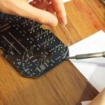
- Highlight the significance of inspection
Inspection of the bare circuit board is one of the key points to reduce the assembly cost. The manual inspection covers basic checks like PCB thickness, the surface finish of the PCB, board warpage, etc. Automated visual inspections can check for track shorts or opens, missing components, and other defects. Catching flaws in the initial stage can save a lot of debugging time. Detailed Bare board inspection before mounting the components is a good consideration for reducing the assembly cost.
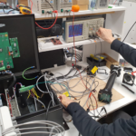
- Choose an experienced and reliable PCB contract manufacturer
With all the above recommendations to reduce the PCB assembly cost, it is of utmost importance to choose an experienced PCB Manufacturer. Researching the background and competence of the assembly provider may be time-consuming but is far more rewarding as some of them have technical teams to assist in:
- Providing standard BoM formats
- Electrical and Mechanical Design support
- Multiple sources for component procurement
- Well-organized Test setups and debug supports
- Expertise in assembly and production
Collaborating with one such PCB Assembly provider will reduce the assembly cost and bring out a superior product to the market.
Many contract manufacturers provide different cost options based on the expected turnaround time. If your product is well planned, then providing sufficient turnaround time to your contract manufacturer can reduce the assembly cost without compromising on the PCB quality.