You can think of noise as an unwanted signal. This signal creates an error by combining with the desired signal in your circuit. Exterior sources can couple into your circuits, such as your 50 or 60 Hz DC mains signal or your cell phone. The starting point in your circuit’s noise evaluation is to reach a theoretical determination of the analog noise levels. In this blog, we will work strictly on analog intrinsic noise.
An amplifier generates voltage and current noise in the 1/f and broadband frequency range. Additionally, the standard resistor generates thermal noise that is flat across the same frequency spectrum. A closed-loop amplifier circuit in a gain of 2 volts per volts (V/V) grows an input signal from ± 1 V to ± 2V at the output (Figure 1).

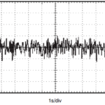
In the top right graph, the input signal is a ± 1V sinusoidal signal. Given an amplifier circuit gain of +2 V/V, the output signal in the middle diagram is a ± 2V sinusoidal signal. In an ideal world, the amplifier and surrounding resistor’s noise is zero. But this is not the case. The bottom Figure 1 graph shows the actual circuit output with a significant amount of intrinsic noise.
Circuit noise sources
Let’s see if we can track down the source of the noise in Figure 1. The next step is to show the amplifier circuit with all amplifier and resistor noise sources. Semiconductor devices and resistors generate predictable intrinsic noise. The Figure 1 amplifier circuit noise comes from the input voltage noise (VA-N) and current noise (VA-I). The resistor noise (VR1_N, VR2_N) contributes to the VOUT total output noise (Figure 2).
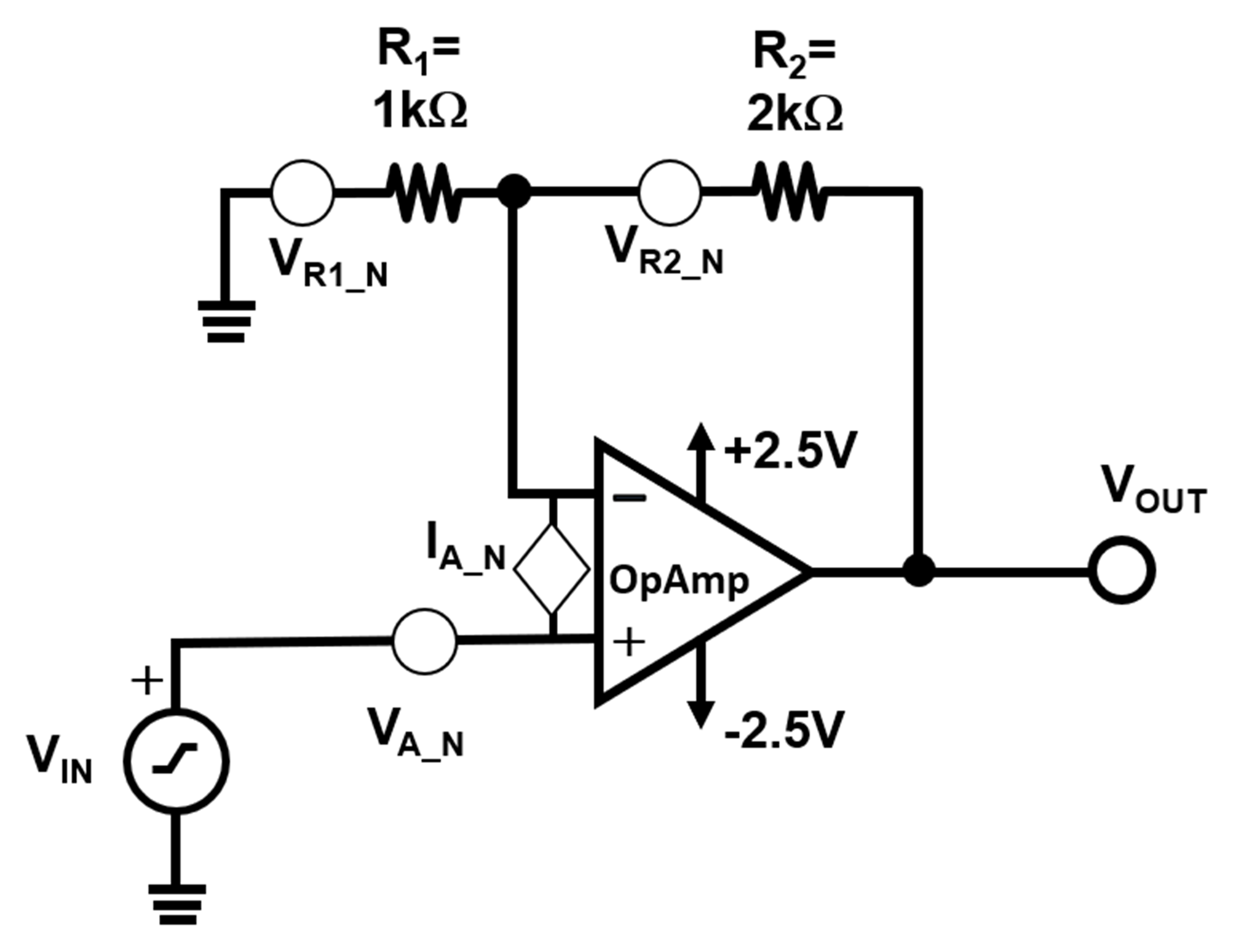
It is important to note that the amplifier voltage noise model is at the non-inverting input of the amplifier. The amplifier current noise flows through R1 and R2, and the amplifier gains the current-resistance voltage to the output of the amplifier.
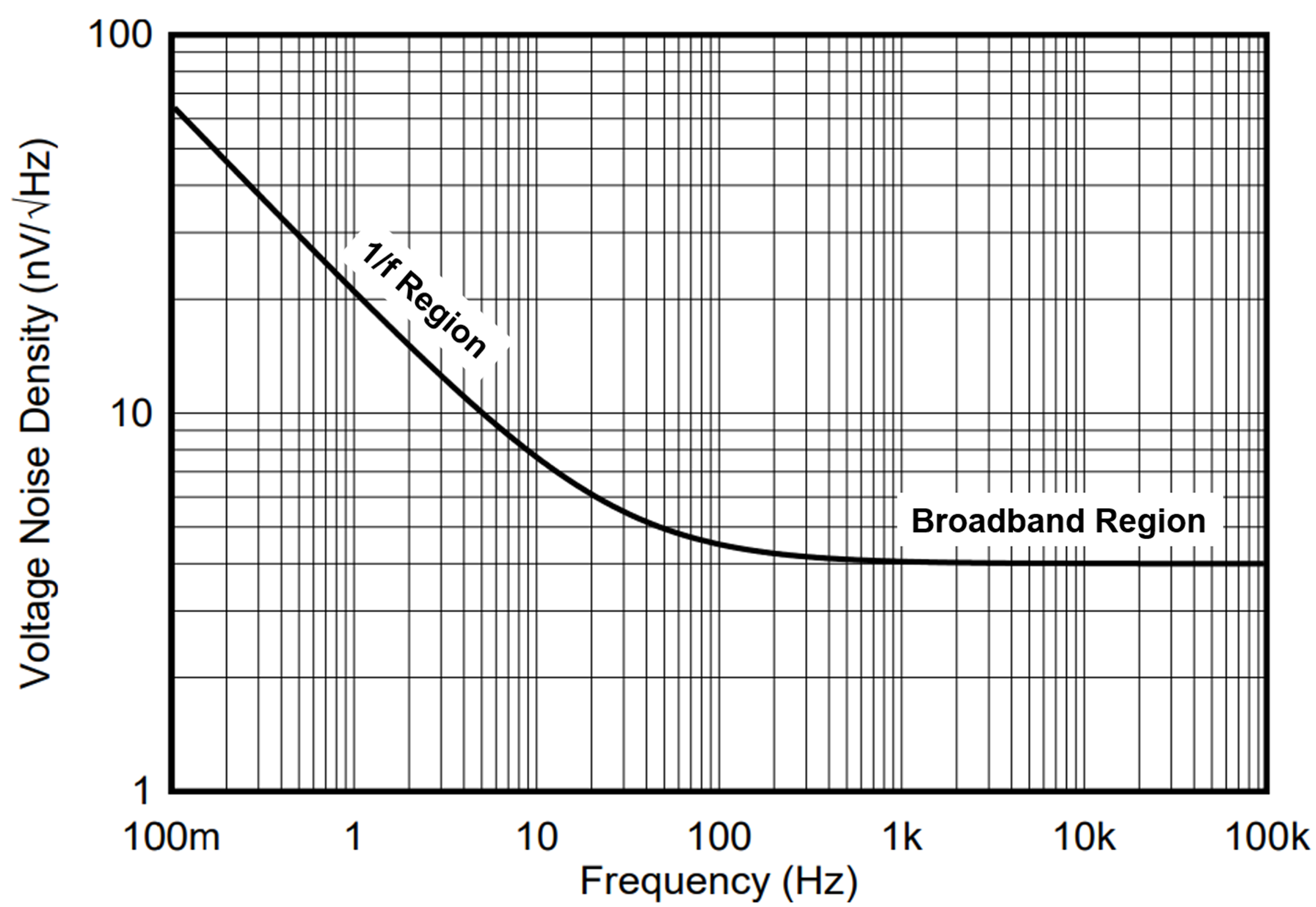
The amplifier’s voltage and current noise have 1/f noise at low frequencies, except for zero-drift amplifiers. Past the 1/f corner frequency, the amplifier produces a broadband noise (Figure 3).
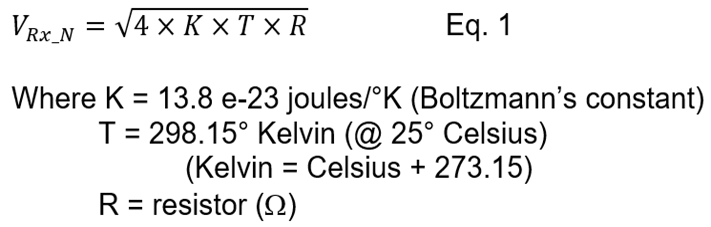
The resistor’s thermal electron agitation sets the conductor’s noise level. The synonyms of the resistor and the broadband noise category are white noise, Johnson noise, thermal noise, and resistor noise. In 1928 J. B Johnson found the conductor’s existing nonperiodic voltage. He also found a temperature related to the magnitude of the conductor’s voltage. The ideal calculated magnitude of the resistance thermal noise voltage is dependent on the Boltzmann’s constant, Kelvin temperature, and resistance value (Equation 1).
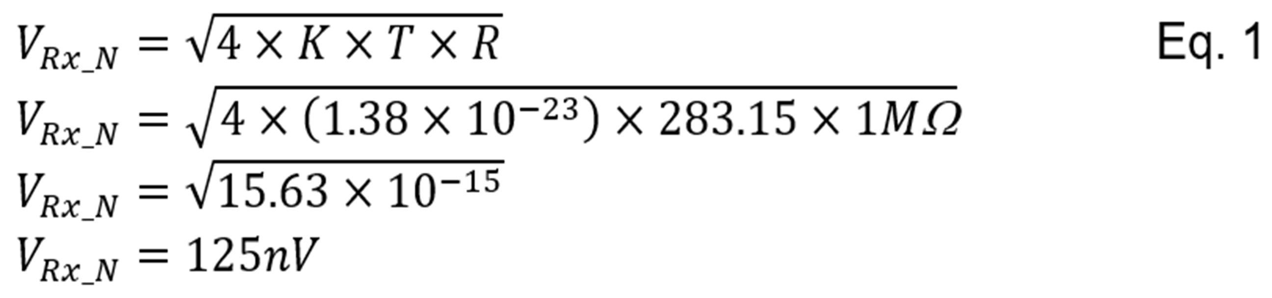
For example, for a Celsius temperature equaling 10°C and a 1 MW resistor, the thermal noise voltage is:
One would hope that you could add the individual noise sources together. That equation makes sense if the signals are correlated. However, noise sources are not correlated, so the appropriate formula for adding noise sources is the square-root-of the-sum-of the-squares (RSS). The equations below summarize the noise calculation of this circuit.
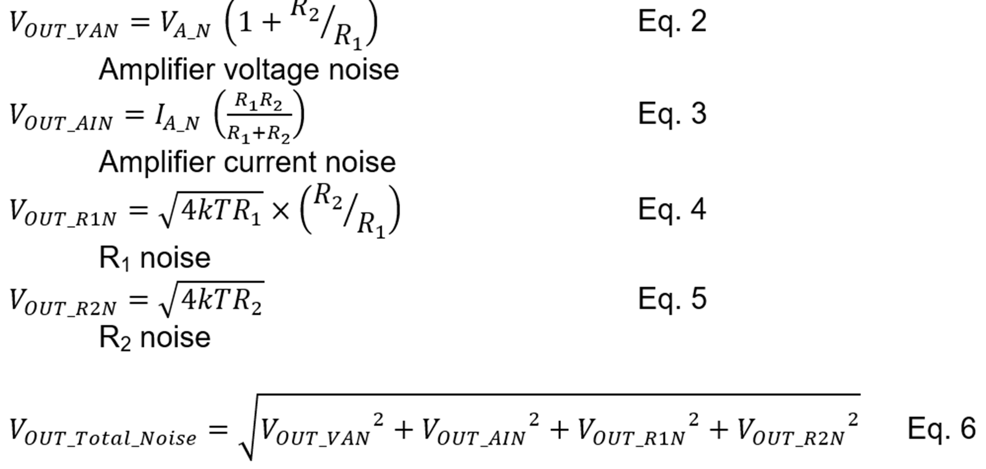
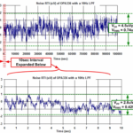
Figure 4 shows an oscilloscope view of broadband or white noise waveform in the time domain when we examine the broadband noise. In general, broadband noise is in the middle-to-high frequency range or frequencies greater than 1 kHz.
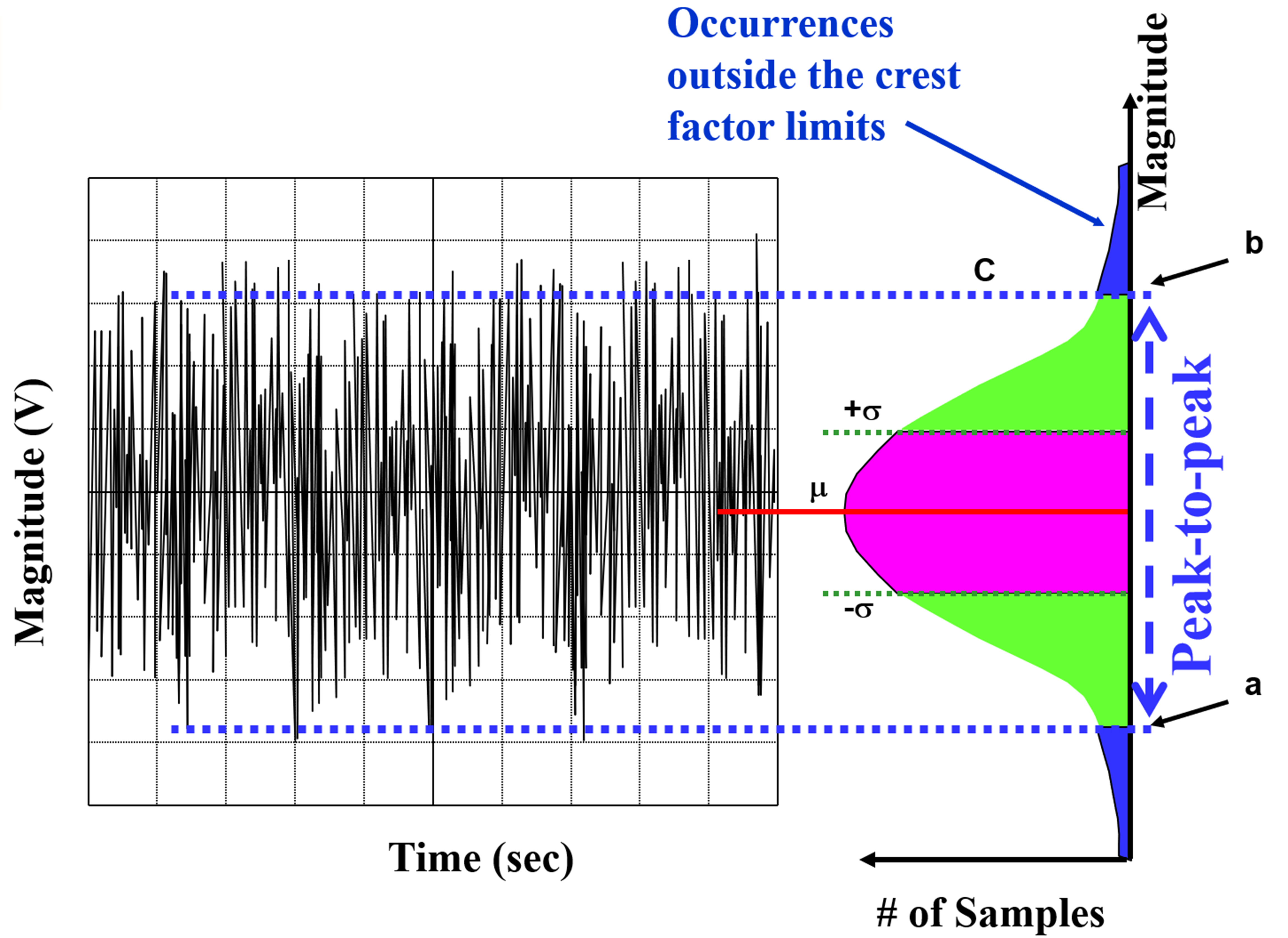
In Figure 4, the right diagram illustrates a normal statistical distribution and represents the cumulation of the data peaks on the left. The labels for the lines are m, s, and C. m equals the mean of all collected signals on the right diagram. The data between the green lines capture ±s (2s) or 68.3% of the samples. The data between the blue lines, C, capture the samples that land between the peak-to-peak (P-P) specification.
The design engineer defines P-P specification, which depends on a particular design requirement. Equation 7 calculates the Figure 4 C limits.
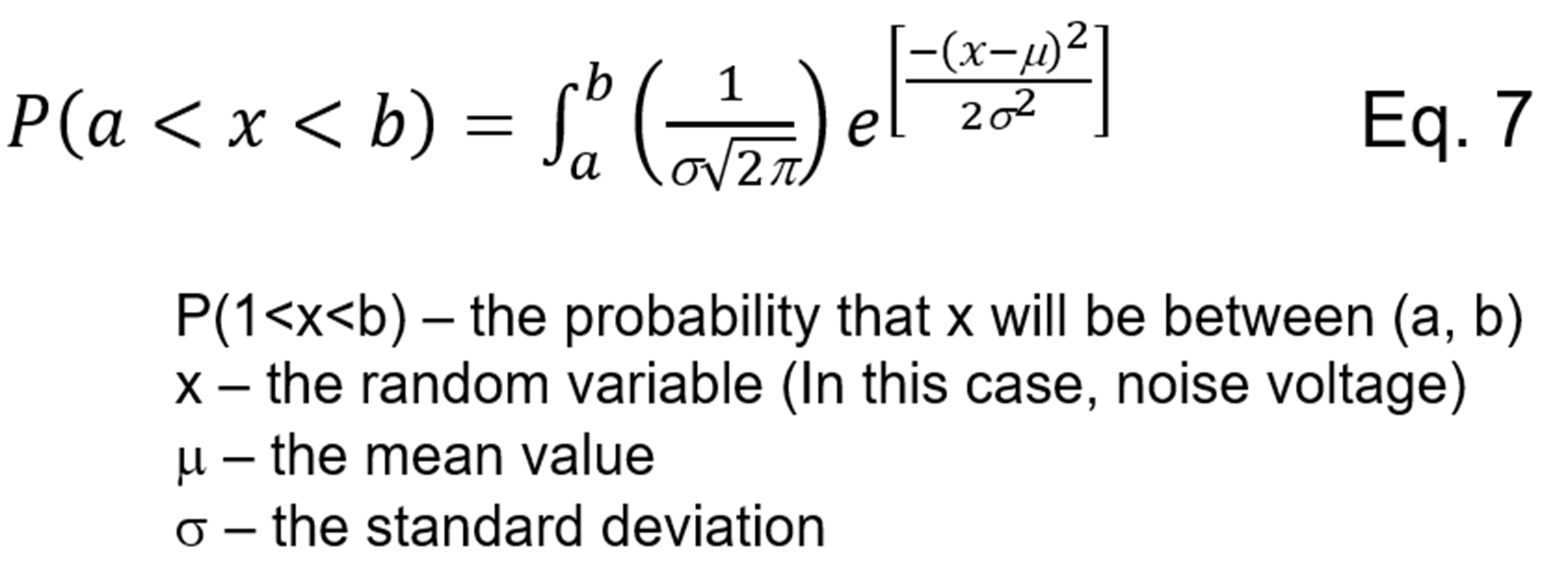
For example, if P(-1<x<+1) = 0.3, the probability that x is between -1 and 1 is 30%.
If the designer prefers an rms response, 2s is appropriate for that application. This choice identifies the data occurrence between the s lines is 68.3% of the time (Figure 5).
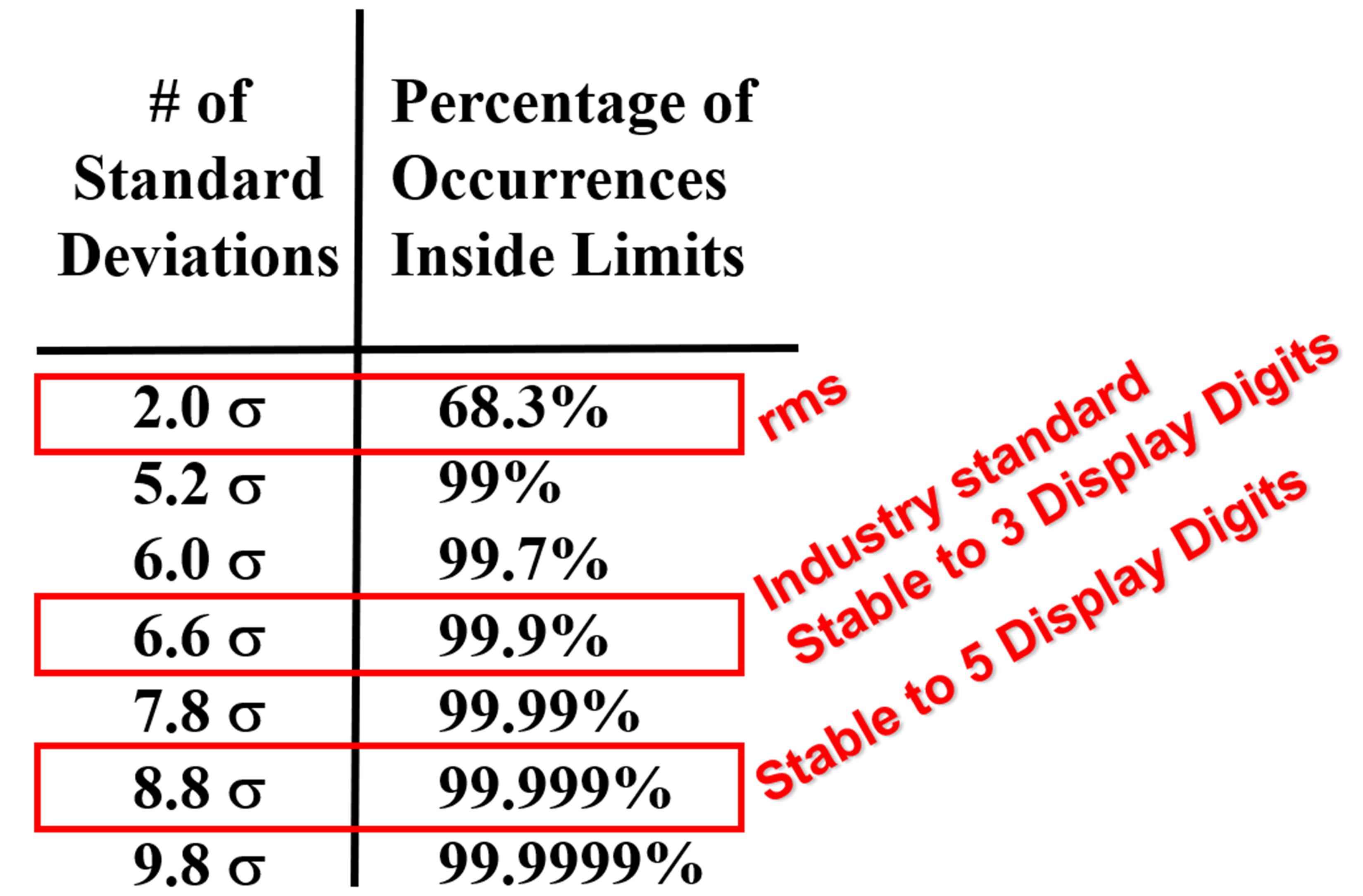
Figure 5 has seven different crest factor limits that show the number of standard deviations per the measurement probability. The industry P-P standard is either 6.0 s or 6.6 s per the product datasheet specifications. Keep in mind that the tails of the Gaussian curve are infinite. There is always a possibility that noise is outside the designer’s “a” and “b” range.
Conclusion
Start your circuit’s noise evaluation by identifying the value of the semiconductor and resistive noise sources. An amplifier generates voltage and current noise across the 1/f and broadband regions. The resistor generates thermal noise that is flat across the frequency spectrum. The noise contribution of these semiconductor and resistive elements combines with the RSS equation.
References
Noise Reduction Techniques in Electronic Systems, Henry W. Ott, John Wiley & Sons, ISBN 0-471-85068-3
“Analysis and Measurement of Intrinsic Noise In Op Amp Circuits Part II: Introduction To Op Amp Noise”, Texas Instruments, Art Kay,
“Squash 1/f noise with zero-drift amplifiers”, Baker, Bonnie, EEWorld
“Including the often overlooked 1/f Current Noise”, Baker, Bonnie, EEWorld, July 28, 2021
“Negotiate through 1/f noise challenges towards sample sizes into the 100s of years” Baker, Bonnie, EEWorld, July 12, 2021