
By unclejed613, “Well-Known Member” on Electro-Tech-Online.
No matter how “digital” things get in modern consumer electronics, when it all comes down to it, after all of the digital magic is done, air must be moved for you to hear the results. An analog voltage and current must be applied to some type of device that displaces air. To displace enough air to cover the whole audio spectrum, at realistic volume levels (and some of us like it real loud….) requires quite a considerable amount of power. As Home Theater systems become bigger and more complex, they also contain more analog amplifiers (I’ll cover Class D, so-called “digital” amplifiers in a separate article).
My goal with this article is for the reader to gain enough knowledge to troubleshoot everything from a discrete headphone amplifier to a kilowatt PA system amp without too much difficulty. Even with the many variations in amplifier designs, they all boil down to a few basic building blocks, no matter how complex it might look on a PC board. Amplifier design and troubleshooting are not based on some “black art”, but are actually quite logical and methodical. My attitude in the work I do is “An amplifier is an amplifier, and no matter how complex, they all follow some basic rules”.
Basic Amplifier Topology
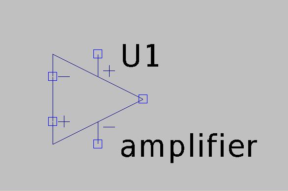
While the schematic one looks at for an amplifier might seem to be an endless sea of silicon and other components, all modern amplifiers are basically a gigantic OP-AMP. They share the same circuit elements as any op amp, and as we go along here you will begin to see the similarities. (FIG 01)
(fig01)
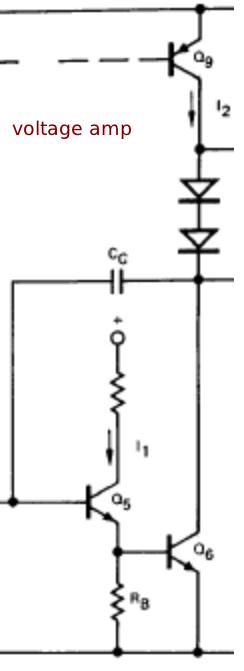
So let’s look at the topology (layout) for an amplifier. In FIG02, we see three stages, an Input stage (or Diff Amp, or LTP (Long Tailed Pair)), a 2nd stage (also known as the Voltage Amplifier Stage or VAS, and a class AB output stage. Actually this diagram is that of an op amp, but as we will see an audio power amp is an oversized copy of the same device.

In the Input stage, we see a pair of transistors with current fed from a common current source at the emitters. There are actually two inputs here, an inverting (-) input and a noninverting (+) input, just like in an op amp. the noninverting input is usually used for the signal input, and the inverting input deals with feedback. In all audio amplifiers, the feedback exists in two distinct forms. DC feedback is applied to keep the DC offset of the amplifier output very small (generally less than +/-50mV). AC feedback sets the overall voltage gain of the amplifier, and minimizes distortion. Just as in an op amp, the inverting input tracks the noninverting input (i.e. you will see an identical copy of the waveform applied to the noninverting input appearing at the inverting input). We see a typical diff amp in fig03.

(fig 03)
Since the emitters of the transistors are fed with a single current, the outputs (in the form of collector currents) are the DIFFERENCE between the collector currents. Usually only one of the collectors is sampled to drive the next stage, but in some designs both currents are used.
The second stage (VAS) is driven by the collector current of the noninverting input transistor. Between the diff amp and the VAS transistor, the waveform does not exist as a voltage signal, but as a current, Keep this in mind, You won’t see much in the way of voltage variations if you measure this signal with an oscilloscope, and even if you do, they will seem to look very distorted. . These current variations are translated by the VAS back into a voltage waveform. Here, on the collector of the VAS is where signals reappear in the form of an amplified voltage. In the example of FIG04, there’s actually a “composite” transistor being used, but it usually exists as a single transistor with the emitter connected to the rail, and the base going to the collector of the input transistor. You will also notice a Compensation Capacitor (Cc in FIG04). This stabilizes the amplifier and keeps it from becoming a large oscillator (more about this later). Notice also that the load for the VAS transistor is a current source. In some amplifiers, this can be a simple resistor, or a “Bootstrap” which is a pair of resistors and a capacitor used to increase the load impedance of the VAS as well as extend the voltage swing. There will be a whole section about current sources. The current source is used here as a high impedance load for the VAS, yet it can supply the required amount of current for the VAS (unlike a large value resistor).
(fig 04)
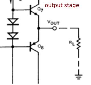
The output stage is a voltage follower buffer. As such it usually has no voltage gain, but has a high current gain.The diodes shown set a bias voltage to keep the output transistors partially turned on. Otherwise, there would be a gap near the zero crossing of the output voltage where there is no output at all. This is called “Crossover Distortion”. In an audio amplifier, the output transistors have low value (0.47 ohms or less) emitter resistors to improve thermal stability, The diodes are usually replaced with a transistor “adjustable zener” circuit, with the transistor thermally coupled to the output transistors. This bias circuit reduces the bias as the temperature rises, at the same rate that the Vbe of the output transistors decreases. This keeps the output transistors from going into thermal runaway and burning out. From the common tie point of the emitter resistors of the outputs is taken the output signal that drives the speaker. The feedback signal is also tapped off at this point.
 (fig 05)
Editor’s Note: Part 2 of Amplifier Theory: Design and Troubleshooting will continue later this week with an explanation of the building blocks of amplifiers: current sources and current mirrors.