
Analog circuits based on op amps can be used to implement mathematical functions and are still useful in many applications due to their unique attributes.
Part 1 of this FAQ looked at the basic need for and virtues of analog-based computational circuits. Part 2 looks at some implementation specifics and considerations.
Q: What are the basic analog building blocks needed?
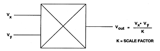
A: The two key analog building blocks are the operational amplifier (op amp) and the analog multiplier. The analog multiplier is a clever arrangement of transistors (now in an IC, of course), with a function which is simple to define: the signal at the output is the product of the two input signals, moderated by a scale factor which may be fixed user selectable (Figure 1). The multiplier can be used to square a signal by feeding the same signal to both inputs, but also much more.
Q: What are some examples of these computation circuits?
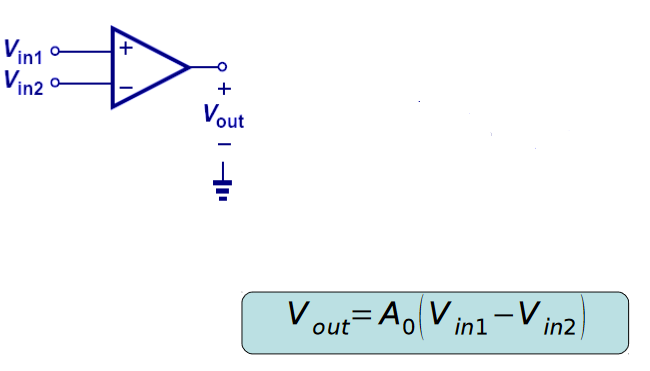
A: A summing circuit is the next basic element (Figure 2). It is based on the standard op amp.
Q: Are there others?
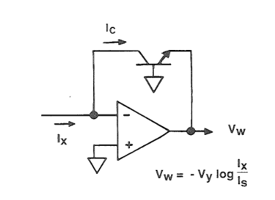
A: There are many! The logarithmic amplifier (log amp) is another valuable analog function, as determining the log of a signal is very calculation intensive (unless a specialized processor core is used) and not practical for high-speed signals or low-level RF, since the log function is needed to adjust the front-end gain of the weak input. There are several ways to build a log function; one of the most common approaches begins with a diode or transistor collector-emitter in the feedback loop path (Figure 3), (but there is much more needed to make a truly viable log amp).
Q: What about other basic functions?
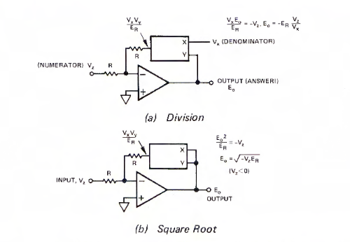
A: Division and square roots are accomplished with a multiplier and an op amp, with fairly simple topologies (Figure 4):
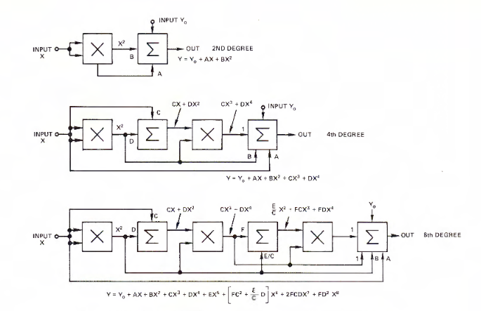
Q: Can more complicated functions be arranged?
A: Yes, these functions can be cascaded for polynomial series expansion of as many degrees as desired, (Figure 5).
Q: Anything else?
A: Other arrangements provide the integration and derivative functions by using a capacitor in different placements around an op amp, and using a diode and capacitor to build a peak detector (again, along with an op amp). The latter function is especially useful and is often embedded deep within in an RF-front end IC, as it is impractical to build a peak detector for RF signals with standard hardware and microprocessor. Doing so would require an RF preamplifier, superfast A/D, and a short but fast-repeating “comparison loop” in software. That’s a very costly, power-hungry, and resource-hogging approach which can instead be accomplished with a few analog components
Q: Can I just build my own analog computation circuits using inexpensive op amps and other basic, passive components?
A: You could in principle do so, but performance would be “marginal” at best. The reality is that the concept is sound and fully proven, but an analog computation block with acceptable performance has many subtleties in hardware execution. There are issues of drift, imbalance, linearity, saturation, stability, dynamic range, offsets, and many more.
For this reason, the best course is to buy an IC which incorporates the complete functional block, often with some user-settable parameters such as gain. Designers of these ICs can take advantage of IC process technology considerations which combining discrete components cannot do, such as using matched resistors with nearly identical drift, or current sources with nearly identical characteristics, to achieve outstanding performance. There are many other subtleties and “tricks” they use as well as fabrication and trim steps that they can employ.
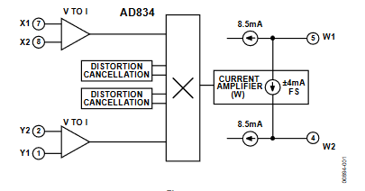
The complete part comes with the datasheet, of course, which fully characterizes the block across many parameters and conditions, and so defines performance over all relevant conditions. An example is the Analog Devices AD834 (Figure 6), a monolithic, laser-trimmed four-quadrant analog multiplier (both inputs can range positive and negative) intended for use in high-frequency applications, with a bandwidth of 500 MHz; the typical total full-scale error is 0.5%.
Even though digital computation is the dominant approach used now for calculation — and with excellent reason — there are many “smaller” situations where an analog computation function is a technically viable, attractive solution to the application requirements. For that reason, good designers look at the system requirements and don’t automatically assume they need to go digital, for some installations.
References
- EE World, “Why Use a Nonlinear Amplifier?”
- International Slide Rule Museum
- The Analog Computer Museum
- The George A. Philbrick Researches Archive
- K2-W Operational Amplifier Data Sheet and Applications
- Robert Paz, “Analog Computing Technique”
- Quora, “What are the advantages analog computers have over digital ones?”
- The Computer Museum, “Analog Computers”
- Analog Devices, “Op Amp Applications”
- Analog Devices, “Multiplier Application Guide”
- Analog Devices, “Analog Multipliers MT-079 Tutorial”
- University of Rhode Island, “Operational Amplifier as A Black Box”
- Analog Devices, “Nonlinear Circuits Handbook”
- Analog Devices, “Amplifier Applications Guide”, Section 9, Section 10