The classic wooden breadboard is obsolete, but its name continues to refer to a vital engineering tool that has changed to meet today’s component and design realities.
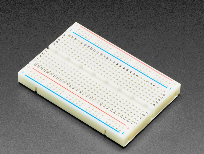
As leaded components such as discrete transistors and low-pin-count ICs in DIP packages came into use in the late 1960s and 1970s, breadboarding technology evolved as well. Among the popular options were “solderless” breadboards which are still available in many configurations (Figure 1). They are convenient, accessible, easy to use, and support a reasonable component density.
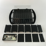
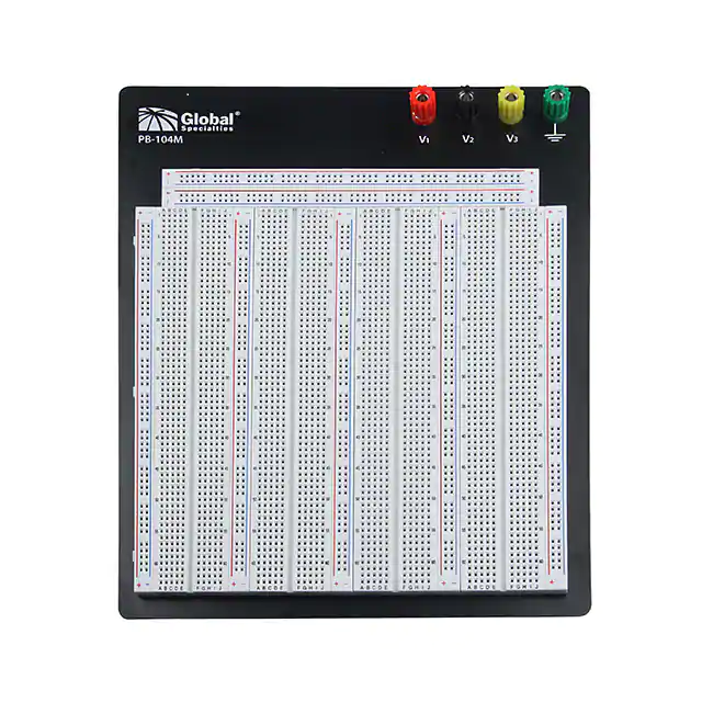
A more advanced example is the PB-104M Externally Powered Solderless Breadboard Assembly from Global Specialties, which is well-suited for prototyping low-frequency circuits (Figure 2). It is mounted in a 21 × 24 cm frame (9.45” L × 8.27” W) and includes 3220 tie-points, four binding posts for connecting power supplies, and supports 28 16-pin ICs; jumpers are made using 0.4 to 0.7-mm diameter wire stripped at the end. The key to the versatility of this breadboard is that the holes are spaced 0.1 “apart to accommodate standard DIP components as well as the pins of adapters and headers, in addition to wire leads.
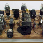
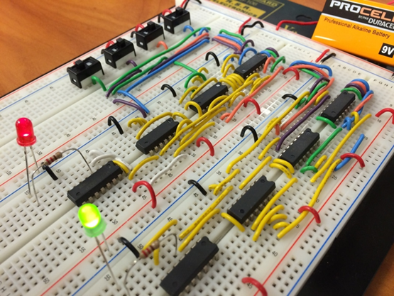
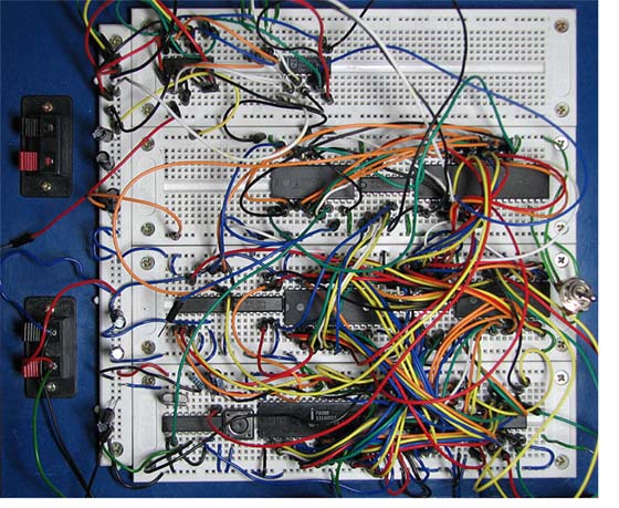
If you do a web search, you’ll see many experimenters still using these for projects based on discrete leaded devices (transistors, LEDs, switches. Depending on the project and the designer, they can be neat and tidy (Figure 3) or evolve into somewhat of a messy arrangement (Figure 4).
The practicality of such solderless breadboards is limited for an obvious and a not-so-obvious reason. The obvious reason is the tiny size and/or high-density nature of many passive and IC components. In some cases, it is possible to substitute a leaded resistor for a chip resistor measuring just a few millimeters on a side. Still, you can’t replace a 100+ lead (often as bumps rather than actual leads), tight-pitch IC with its lower-density counterpart. In fact, even many of the latest low-pin-count ICs, such as 8-lead op amps, are only offered in tiny surface-mount (SMT) packages without DIP counterparts.
But there’s a second, less-obvious reason why such traditional breadboarding is no longer feasible or even desirable. Before microcontrollers, microprocessors, high-functionality ICs, and software “took over,” analog and basic digital circuits had a linear signal flow from input to output. For example, a public-address system amplifier would have a preamplifier stage to interface with the microphone, followed by filter stages to shape the response and attenuate noise, then a low-level power amplifier/driver to boost the signal, and finally, a power amplifier to deliver the higher-power output for the speakers.
In that typical design process, these stages would be built, tested, and added to each other in sequence while checking signal flow at and through each stage to ensure there were no unintended interactions in overall signal flow and integrity and similar; there was an analogous situation for basic digital-logic ICs as they “processed” a signal.
Now, however, a typical system consists of high-functionality blocks which interact with each other and, most critically, with the system processor. There is a significant amount of back-and-forth signal, and data flow among all these blocks which can range from a low-speed, highly sensitive sensor amplifier to an RF link for Wi-Fi or Bluetooth, as well as the user interface other I/O. There is no single flow path from input to output; instead, it is a web-like topology with the various elements linked to each other.
This arrangement of signal paths calls for a different approach to development, debug, and test and therefore calls for different breadboard tools, which will be discussed in Part 3.
EE World Related content
Mounting base kit simplifies electronic prototyping tasks
Understanding delay for I/O: Using Arduino functions vs. coding the MCU
Plug-And-Play Diagnostic Devices
Considerations in PCB layout guidelines
Getting started in electronics: core components
What is a Board Support Package?
A “canned” module/IC solution simplifies wireless implementation, but potential design-in issues remain
External references
Wikipedia, “Fahnestock clips”
Schmartboard Breadboard Systems
Phase Dock Inc., Universal WorkBench system