• Skip to primary navigation
  • Skip to main content
  • Skip to primary sidebar
  • Skip to footer

Analog IC Tips

Analog IC Design, Products, Tools Layout

  • Products
    • Amplifiers
    • Clocks & Timing
    • Data Converters
    • EMI/RFI
    • Interface & Isolation
    • MEMS & Sensors
  • Applications
    • Audio
    • Automotive/Transportation
    • Industrial
    • IoT
    • Medical
    • Telecommunications
    • Wireless
  • Learn
    • eBooks / Tech Tips
    • FAQs
    • EE Learning Center
    • EE Training Days
    • Tech Toolboxes
    • Webinars & Digital Events
  • Resources
    • Design Guide Library
    • Digital Issues
    • Engineering Diversity & Inclusion
    • LEAP Awards
    • Podcasts
    • White Papers
  • Video
    • EE Videos
    • Teardown Videos
  • EE Forums
    • EDABoard.com
    • Electro-Tech-Online.com
  • Engineering Training Days
  • Advertise
  • Subscribe

CAD package handles IC, package, and PCB design

March 23, 2015 By Lee Teschler Leave a Comment

A new software package enables what is called the co-design of ICs, packages, and the printed circuit boards on which they reside. Called the Xpedition Package Integrator, the software is said to facilitate the planning, assembly and optimization of today’s complex multi-die packages. It incorporates a special virtual die model concept for optimizing IC-to-package connections. The overall aim is to let designers plan, assemble and optimize complex systems with minimal source data. The new Package Integrator flow is said to let
design teams realize faster and more efficient physical path-finding and seamless tool
integration for rapid prototyping.

mentor graphics xpedition
The Xpedition Package Integrator is said to let uses manage connections of boards, chips, and packaging in one environment.

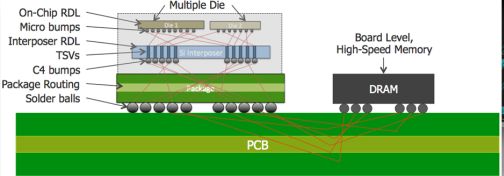
ICs, packages and PCBs are optimized with each other to reduce package substrate and PCB costs by efficient layer reduction, optimized interconnect paths, and streamlined/automated control of the design process. The Xpedition Package Integrator product also is said to provide the industry’s first formal flow for ball grid array (BGA) ball-map planning and optimization based on an “intelligent pin” concept, defined by user rules. In addition, a multi-mode connectivity management system (incorporating hardware description language (HDL), spreadsheet and graphical schematic) provides cross-domain pin-mapping and system level cross-domain logical verification.

multiple target platforms
Designers can consider multiple target platforms (PCB form factors) while planning chip/package connections and their optimization.

The software also provides a cross-domain interconnect visualization in a single view and includes multi-mode physical layout tools with routing for designs of PCBs, MCMs, SiPs, RF, hybrid, and BGA devices. The package works with CFD tools and with software that checks substrate fabrication and signal integrity. Another package enables the simulation of electromagnetic fields for chip-package-board combinations.

The Xpedition Package Integrator comes from Mentor Graphics Corp., Wilsonville, Ore., www.mentor.com/pcb/package-integrator.

Filed Under: PCB design, Software Tagged With: mentor

Reader Interactions

Leave a Reply Cancel reply

You must be logged in to post a comment.

Primary Sidebar

Featured Contributions

High-Performance GPUs Are Located in a Variety of Environments, including Data Center Racks.

AI’s demand for faster, more reliable IC testing

Design a circuit for ultra-low power sensor applications

Active baluns bridge the microwave and digital worlds

Managing design complexity and global collaboration with IP-centric design

PCB design best practices for ECAD/MCAD collaboration

More Featured Contributions

EE TECH TOOLBOX

“ee
Tech Toolbox: Connectivity
AI and high-performance computing demand interconnects that can handle massive data throughput without bottlenecks. This Tech Toolbox explores the connector technologies enabling ML systems, from high-speed board-to-board and PCIe interfaces to in-package optical interconnects and twin-axial assemblies.

EE LEARNING CENTER

EE Learning Center
“analog
EXPAND YOUR KNOWLEDGE AND STAY CONNECTED
Get the latest info on technologies, tools and strategies for EE professionals.

EE ENGINEERING TRAINING DAYS

engineering

RSS Current EDABoard.com discussions

  • PWM or potentiometer to control speed on saw
  • STM32 multiprocessor communication UART
  • analyzing current limiting switch circuit
  • Primary current sense in LLC
  • kit iron soldering question

RSS Current Electro-Tech-Online.com Discussions

  • CR2/CR123A Batteries In Projects
  • Arduino standalone minimal
  • analog logic of shmidt trigger bjt circuit
  • Convenient audio FFT module?
  • Harman Kardon radio module BMW noise
“bills

Footer

Analog IC Tips

EE WORLD ONLINE NETWORK

  • 5G Technology World
  • EE World Online
  • Engineers Garage
  • Battery Power Tips
  • Connector Tips
  • EDA Board Forums
  • Electro Tech Online Forums
  • EV Engineering
  • Microcontroller Tips
  • Power Electronic Tips
  • Sensor Tips
  • Test and Measurement Tips

ANALOG IC TIPS

  • Subscribe to our newsletter
  • Advertise with us
  • Contact us
  • About us

Copyright © 2026 · WTWH Media LLC and its licensors. All rights reserved.
The material on this site may not be reproduced, distributed, transmitted, cached or otherwise used, except with the prior written permission of WTWH Media.

Privacy Policy