Class D amplifiers were first proposed in the 1950s. Why have they only recently been gaining more widespread popularity? The answer involves several factors: There were no switching transistors that met the performance demands of Class D amplifiers until the 1980s. And it was not until the mid-1990s that Class D integrated circuits became available. A typical Class D amplifier will operate at a 250kHz or higher switching frequency. During the 1990s, the combination of dedicated ICs and continued improvements in silicon-based power MOSFETs contributed to an acceleration in the adoption of Class D in high-end audio systems.
Even more recently, high-performance Class D amplifiers have benefited from the development of GaN power transistors. And filterless Class D amplifiers have been developed for more cost-sensitive and lower-power applications where lower-quality audio performance is acceptable. These filterless designs save on cost and board space by eliminating the output LC filter section.
Decreasing Class D tradeoffs
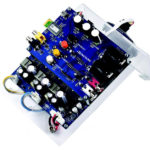
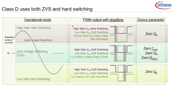
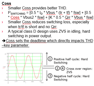
While Class D amplifiers are inherently more efficient than Class AB amplifiers, an acceptable level of total harmonic distortion + noise (THD+N) for Class D amplifiers has not always been easy to achieve. Class D amplifiers use a combination of hard switching and zero-voltage switching and place-specific demands on switching devices. When implemented using silicon MOSFETs, the performance of Class D amplifiers is limited by inherent device characteristics.
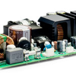
For example, the body diode in a silicon MOSFET is a source of switching noise that negatively impacts the THD+N figure of the amplifier. Silicon MOSFET conduction losses can be reduced by using a larger die size device. But the larger die results in higher gate and output capacitances, increasing switching losses and reducing the efficiency of the amplifier. This can also necessitate the use of a heatsink, increasing size, and adding to cost.
The absence of a body diode in GaN power switches eliminates a significant source of switching noise resulting in cleaner switching. GaN transistors eliminate Qrr and offer a large reduction in Coss to ensure that higher switching frequencies can be used while delivering superior THD+N results. The inherently low RDS(on)(max) in a small package (in contrast with silicon, with GaN RDS(on) can be reduced while shrinking the die size ), ensures that Class D GaN-based amplifiers will eventually provide high audio fidelity in volumes smaller than their Si equivalents and without the need for bulky and heavy heat-dissipating solutions.
Driving out distortion
A problem with early Class D amplifier designs was high transient intermodulation distortion (TIM). The use of silicon MOSFETs, with switching noise, relatively high RDS(on), and high stored gate charge made it difficult to reduce TIM. Class D amplifiers used large levels of feedback to compensate for these shortcomings in the power switches. However, the use of excessive feedback can reduce the quality of the output signal and produce lower quality sound.
As described above, the use of GaN switches addresses most of the concerns with silicon MOSFET switching performance and results in much lower TIM levels. However, GaN devices are still more costly than their silicon counterparts. That currently limits the use of GaN to mostly high-performance designs.
A more difficult-to-address cost is that associated with the output or “reconstruction” filter. This low-pass filter is a critical design element. The audio performance of the amplifier is dependent on the quality and linearity of the filter. The filter performs two critical functions: it reconstructs the audio information for the speaker, and it must attenuate the high-frequency switching component of the Class D output signal.
Filterless Class D amplifiers have been developed for lower performance applications that rely on the inherent inductance of the speaker load to recover the audio signal. The speaker resistance and inductance form a 1st-order lowpass filter. With many speakers, this inherent low-pass filtering is enough to recover the audio signal and prevent excessive amounts of high-frequency switching energy from being dissipated in the speaker resistance.
Controlling EMI and other design and specification considerations for Class D amplifiers will be discussed in more detail in the third and final installment of this FAQ series, “Sound Design Considerations for Class D Amps.”
References
Class D audio amplifiers: what, why and how, Analog Devices
Class D Audio Amplifiers, Efficient Power Conversion
Class D audio using the PE29102, pSemi
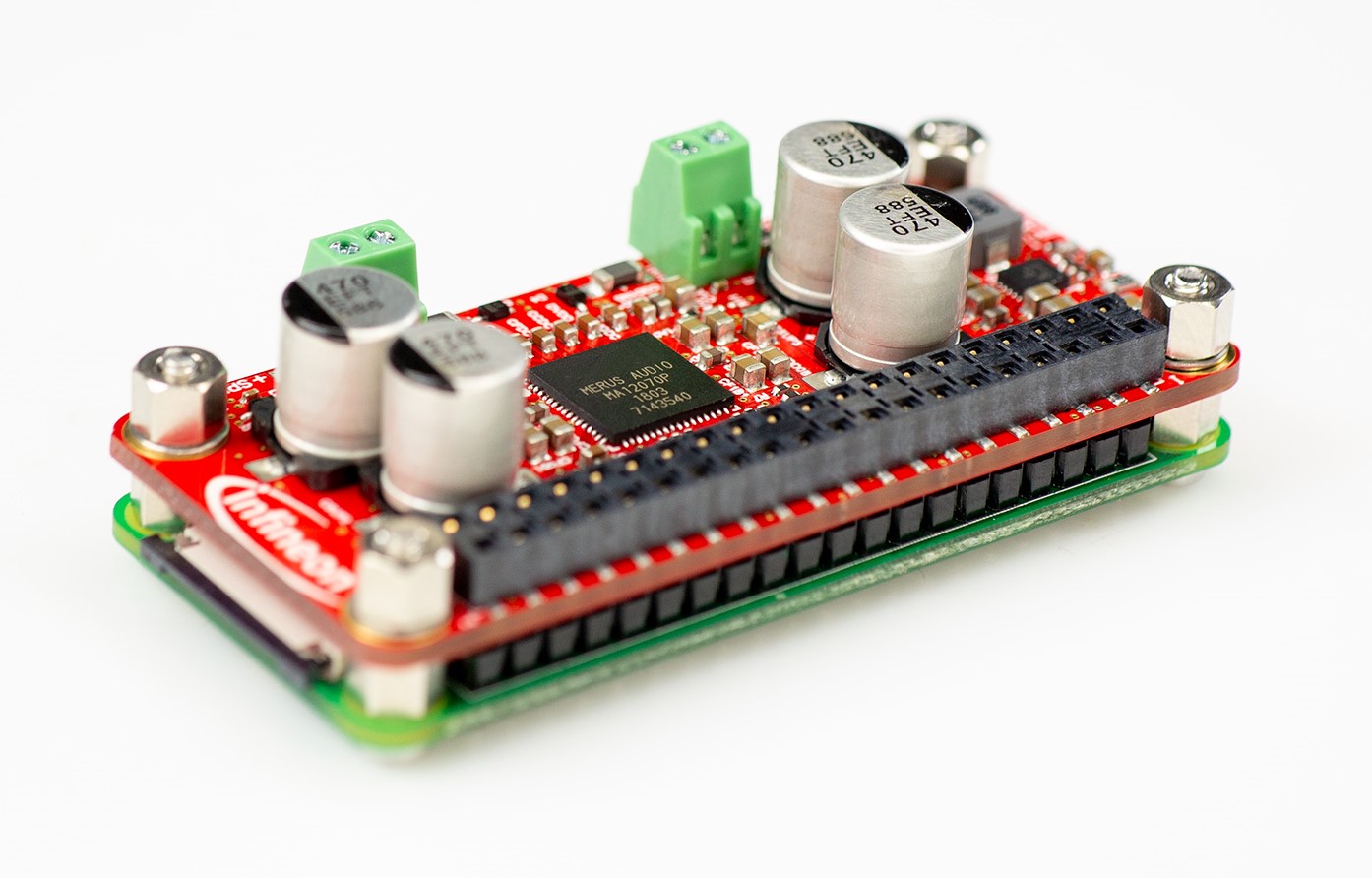
Class D 40W audio amplifier Raspberry Pi hat, Infineon
Fundamentals of Class D Amplifiers, Maxim Integrated Products
Class-D amplifier, Wikipedia