• Skip to primary navigation
  • Skip to main content
  • Skip to primary sidebar
  • Skip to footer

Analog IC Tips

Analog IC Design, Products, Tools Layout

  • Products
    • Amplifiers
    • Clocks & Timing
    • Data Converters
    • EMI/RFI
    • Interface & Isolation
    • MEMS & Sensors
  • Applications
    • Audio
    • Automotive/Transportation
    • Industrial
    • IoT
    • Medical
    • Telecommunications
    • Wireless
  • Learn
    • eBooks / Tech Tips
    • FAQs
    • EE Learning Center
    • EE Training Days
    • Tech Toolboxes
    • Webinars & Digital Events
  • Resources
    • Design Guide Library
    • Digital Issues
    • Engineering Diversity & Inclusion
    • LEAP Awards
    • Podcasts
    • White Papers
  • Video
    • EE Videos
    • Teardown Videos
  • EE Forums
    • EDABoard.com
    • Electro-Tech-Online.com
  • Engineering Training Days
  • Advertise
  • Subscribe

Cloud-based PCB design software helps share layouts and models

February 21, 2020 By Aimee Kalnoskas Leave a Comment

Altium has launched a new cloud-based application that redefines the way that printed circuit board designs are shared between designers, part suppliers, and manufacturers.

The A365 Viewer, powered by the Altium 365 cloud platform, is a brand new, and innovative way to view and share electronic designs through a browser on any web-enabled desktop, phone or tablet. Schematics, PCB layout, and 3D visualization provide an interactive eCAD experience with no downloads or installations required. The A365 Viewer is part of Altium’s cloud strategy and newly launched Altium 365 cloud platform.

A365 Viewer
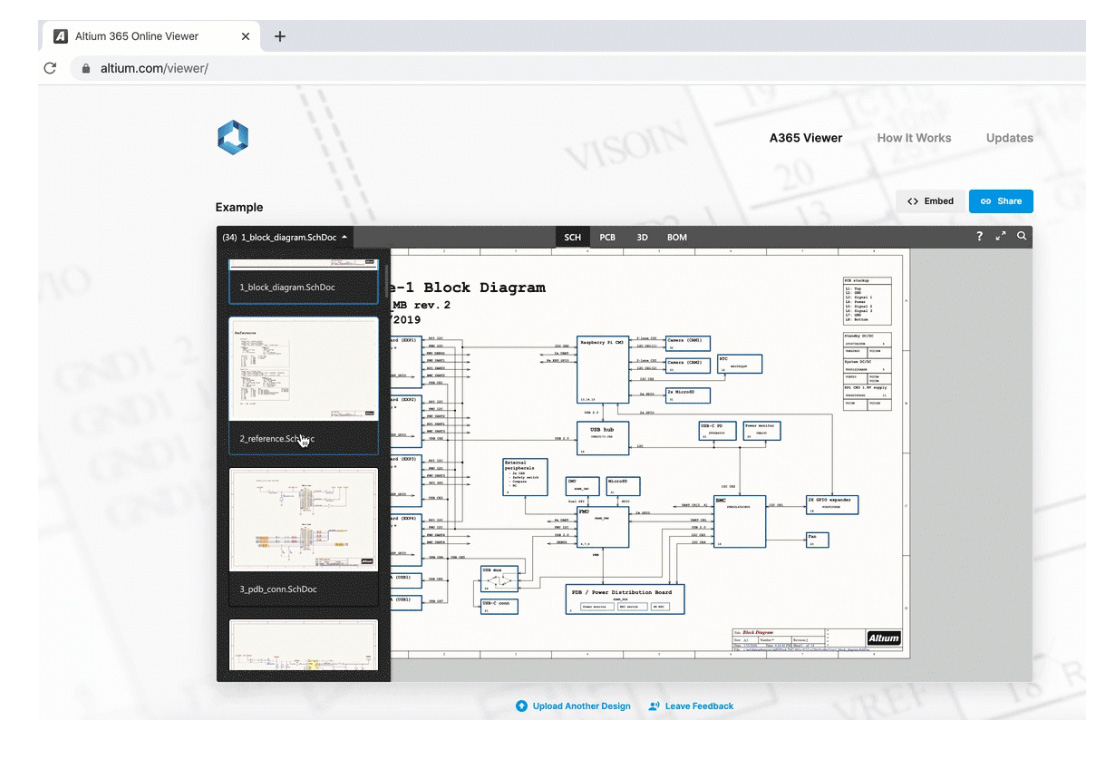
Until now, designers have been forced to share their PCB designs through PDFs or static images. With the new A365 Viewer, an interactive experience is created that retains all of the key relevant information that’s typically lost when sharing static files. For example, the A365 Viewer allows users to search for, select, cross-probe and inspect components and nets while moving seamlessly between schematic, PCB and 3D views of their board.

Using the A365 Viewer requires no CAD tools or experience. The A365 Viewer is designed to work with multiple eCAD formats, currently supporting Autodesk®️ Eagle™ and Altium Designer™.  Other popular PCB design software formats will be supported in the near future.

Anyone can easily embed the viewer on their website, free of charge, by visiting https://www.altium.com/viewer/ . As an example, a well-known developer of electronics hardware and software kits, Arduino, is helping engineers and makers to easily and quickly visualize the PCB designs and assemblies available in their product kits, by embedding the A365 Viewer on the Arduino website.

The A365 Viewer protects the IP rights of design owners while retaining the CAD design details via a new process called Published Design Impression (PDI). The Viewer processes the design source files to create a Published Design Impression, or PDI. The PDI is a CAD-aware, perishable snapshot of the design that captures limited information such as components, net connectivity and basic geometrics, excluding design primitive data that would be required to fully comprehend and author changes to the design.

The design sources are discarded immediately after being used solely for the purpose of creating a PDI. The design is available for the duration of the user’s browser session and is automatically removed when the browser tab is closed.

You may also like:


  • The basics of FR-4 Printed Circuit Boards
  • FR-4
    Printed Circuit Boards, Part 4: Beyond FR-4
  • Vias and multilayer boards
    Printed Circuit Boards, Part 3: Vias and multilayer boards
  • Printed Circuit Boards
    Printed Circuit Boards, Part 1: Context and phenolic boards

Filed Under: Featured, PCB design Tagged With: altium

Reader Interactions

Leave a Reply Cancel reply

You must be logged in to post a comment.

Primary Sidebar

Featured Contributions

Design a circuit for ultra-low power sensor applications

Active baluns bridge the microwave and digital worlds

Managing design complexity and global collaboration with IP-centric design

PCB design best practices for ECAD/MCAD collaboration

Open RAN networks pass the time

More Featured Contributions

EE TECH TOOLBOX

“ee
Tech Toolbox: Test & Measurement
We’ve gathered articles that include hands-on product tryouts and reviews. Indeed, every article in this issue uses an oscilloscope in one way or another so you might just call this “The Oscilloscope Tech Toolbox.”

EE LEARNING CENTER

EE Learning Center
“analog
EXPAND YOUR KNOWLEDGE AND STAY CONNECTED
Get the latest info on technologies, tools and strategies for EE professionals.

EE ENGINEERING TRAINING DAYS

engineering

RSS Current EDABoard.com discussions

  • AASD Controler
  • Help me (amplifier, suggest how to improve)
  • Monostable circuit to always give a 4us pulse..
  • Simulation Issues of PIN Diodes in HFSS
  • SiC FETs in direct parallel in PFC stage

RSS Current Electro-Tech-Online.com Discussions

  • My Advanced Realistic Humanoid Robots Project
  • Hitachi SuperScan Elite 802 CRT Monitor Issues (Model CM802U)
  • Sanity Check – Peltier "Cooler" for Heating and Cooling
  • Funny Images Thread!
  • I am ready to move from electrical and electronics field but confused where ?
“bills

Footer

Analog IC Tips

EE WORLD ONLINE NETWORK

  • 5G Technology World
  • EE World Online
  • Engineers Garage
  • Battery Power Tips
  • Connector Tips
  • EDA Board Forums
  • Electro Tech Online Forums
  • EV Engineering
  • Microcontroller Tips
  • Power Electronic Tips
  • Sensor Tips
  • Test and Measurement Tips

ANALOG IC TIPS

  • Subscribe to our newsletter
  • Advertise with us
  • Contact us
  • About us

Copyright © 2025 · WTWH Media LLC and its licensors. All rights reserved.
The material on this site may not be reproduced, distributed, transmitted, cached or otherwise used, except with the prior written permission of WTWH Media.

Privacy Policy