Digital-to-analog converters (DACs) are subject to gain and offset error. Errors can be compensated for with hardware by using external components or by trimming the DACs after they have been manufactured. Trimming is necessary because the error is caused by mismatched resistors; trimming attempts to change resistor values in the DAC. However, some DACs can be prohibitively tedious due to the high number of resistors. Software methods can also be employed to compensate for DAC errors, but first let’s examine how to determine how much offset and gain error for your DAC.

What is Offset Error?
The ideal transfer function of a DAC is like a slope-intercept equation that you may have first seen in 8th grade math: y = mx + b, where m is the slope of the function, and b is the point where the line intercepts the y-axis (called the y-intercept). The transfer function of an ideal DAC will have no offset and no gain. In reality, there will be some error in an actual DAC, and two that have a direct relationship with the slope-intercept equation are offset error and gain error.
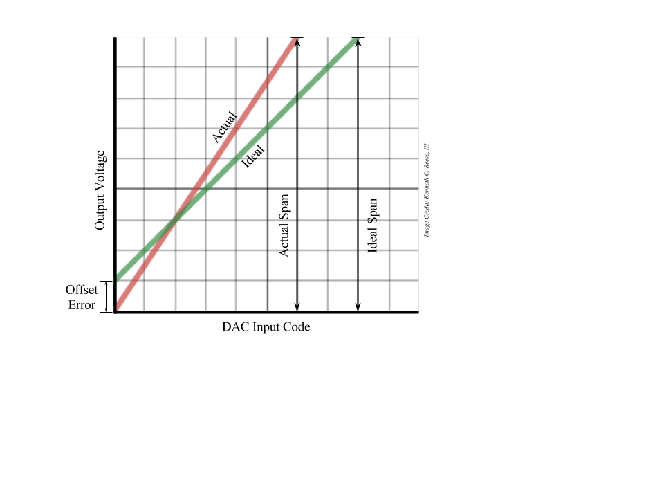
Offset error shifts all points on the output from what would be the ideal transfer function (see Fig. 2). Offset error is much like the b intercept in that transfer equation. Offset error is based on a measurement between two points (at around 90% and 10% of full-scale range) covering the linear operating region of the DAC. In effect, if you feed a DAC an input of digital zero, an offset error causes the DAC’s output voltage to be something other than zero. Since the offset error is consistent in the linear region, it can be compensated for (using software) by adding (or subtracting) the same value to the DAC’s input. If you have a DAC with 2N possible codes and an output span of V volts, then: 1LSB = V/2N volts. How much total offset you have in volts, divided by 1 LSB (in volts) yields the total number of LSB to write to the DAC.
Example:
A 16-bit DAC has 216 = 65536 possible codes. If the DAC’s output span is 12.06V, then one LSB is: 12.06V/65536 = .184mV
If the offset voltage is measured at – 10mV, then the offset value is 10mV, and the offset voltage is equivalent to 54 LSB because 10mV/.184mV = 54 LSB.
Writing 54 LSB to the DAC yields an output of zero volts. To compensate, you will add 54 LSB to the input of the DAC.
Gain Error
If offset error is the y-intercept (b) in the transfer function equation (y = mx + b), then gain error is the m, for slope. Gain error shows up as a deviation from the slope of the ideal transfer function for the DAC. The amount of gain error is measured in Least Significant Bits (LSBs) or as “percent full-scale range” (%FSR) of the DAC. Gain error can be compensated for by calibrating with software or hardware. LSB for a DAC is not the same as the bit with the least weight in a string of bits; that’s a different LSB. For DACs, the LSB is defined as the full-scale voltage range of the DAC divided by 2N, where N is the resolution of the DAC. Therefore, for a 16-bit DAC with a full-scale voltage of 5v: 1 LSB = (5v/216)= 76µV. Gain error is also taken from the 10% — 90% linear operating range of the converter. Gain error exists in all precision DACs. One way to compensate for gain error is to multiply the DAC’s digital input by a value that is the reciprocal of the gain error.
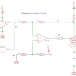
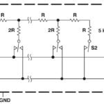
Multiplying DACs (MDACs) do not have an offset error, at least they don’t until you add an operational amplifier at the MDAC’s output, since MDACs are effectively ladders of resistors.
Compensating for error by performing mathematical functions on the input of each DAC may be more calculation-intensive than you had bargained for. Some DACs may have integrated registers for compensation to offload a microcontroller or you can look for precision DACs that have been trimmed post-manufacture.