 by Ken Ghadia, Sales Engineer, TechnoTronix
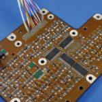
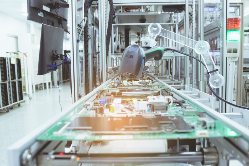
PCB fabrication is transforming circuit board design into a physical PCB based on design specifications. It is usually an outsourced activity done by a Contract Manufacturer (CM) who strictly follows the specifications provided by the designer. Certain critical factors like choice of the PCB substrate, layout strategy, surface coating requirements are decided before fabrication that may impact manufacturing yield and product performance. Hence, understanding the PCB fabrication process and its trends is very important for any PCB designer and manufacturer.
The rising demand for digitization in consumer and industrial electronics is driving many innovations in the PCB manufacturing process. The availability of advanced PCB substrate materials like epoxy and polyamides supports the global PCB market requirements. Recycling of PCBs is considered significant now to meet the environmental and sustainability guidelines set by the government authorities.
The communications and automotive industries are the major applications driving the global PCB market. Technologies like AI, the IoT , and 5G mobile communication also impact PCB manufacturers to bring out revolutions in PCB design and manufacturing technology. Here, we discuss the latest PCB design and fabrication trends that are expanding to meet the technological breakthroughs efficiently.
Flexible PCBs
One of the rapidly growing trends in PCB Fabrication is the usage of flexible PCBs, as they mold into any shape or size. The advantages of Flex PCBs include smaller size, higher flexibility, and multiple substrate options. These features make them the best fit for medical, wearable, and other application-specific requirements. Apart from Flex PCBs, there are Rigid-flex PCBs used for compact product development.
High density interconnect
Automation in every sector has resulted in a deliberate need for high-density interconnect (HDI) PCBs as they offer reliable and high-speed signal transmission. HDI PCBs provide smaller trace width that improves the wiring density. The reduced PCB layer count decreases production cost as well. Thus, HDI PCBs are essential in smart applications like aerospace, medical, and wearable tech devices.
High power boards
With the focus on renewable energy sources like solar power, the demand for high-power PCBs is growing considerably. Most solar panels operate in the range of 24 V to 48 V Also, the interest in electric vehicles adds to the requirements of high-power boards. Accommodating long-lasting battery packs would allow a product to operate for a longer duration, which calls for a high-power board design with an efficient thermal design for heat dissipation.
PCB autoplacers
The PCB design technology also optimizes for higher efficiency by introducing autoplacers and autorouters in EDA tools. This automation is speeding up the design to market time with improved quality. Going forward, CAD systems will be integrated with the process to increase the design and simulation speed to a large extent.
Smart device demand
The demand for smart devices is ever growing with the trends of connecting smartphones with smart homes or smart offices. Scalable and securely connecting devices are required for such applications. This could be a great revenue generator in the future and hence asks for the flexibility and adaptability of the PCB manufacturers to capture the market.
COTS components
These are the ready-made, assembly, or part-designed products used in commercial applications to speed up the design process and other benefits. They make an excellent choice for critical and space-based systems as they meet stringent standardization and regulation guidelines. Further, they offer reliability and efficiency with a lower overhead. The aerospace industry uses the COTS components widely, and other domains may soon catch up with the trend.
Component supply chain control
With new applications on the horizon, there is plenty of opportunity for the introduction of fresh components. Already there is a growing need to eliminate counterfeit components from the supply chain. This is highly necessary for critical applications like medical equipment, artificial intelligence, virtual reality, etc. New PCB manufacturing methods are required to control this problem, such as implanting a tiny chip inside components to make the possibility of fake components too complex.
IoT PCBs
IoT devices are compact, portable, and reliable, driving PCB manufacturers to incorporate safety features against tampering. IoT PCBs have to follow specific standards and regulations to comply with the security required.
Biodegradable PCBs
Disposing of the traditional PCB is harmful as it contains a lot of chemicals that are not degradable. Disposed PCBs contribute to electronic waste adding to the global concern of e-waste management. The new trend of biodegradable PCBs is one solution to this e-waste problem. Options such as extracting metals from e-waste are also considered, which can be reused through the refining process. Biodegradable substrate materials are evaluated as safe alternatives and may help avoid chemical etching in the PCB assembly process and reduce manufacturing costs.
PCB board cameras
Board cameras are catching on in both consumer and industrial electronics. A small camera is mounted directly on a PCB in order to take pictures and videos. Some of the applications of board cameras may be handheld mobile devices in consumer electronics, tiny medical equipment used in non-invasive procedures, and surveillance devices used for monitoring and security purposes.
Many more potential innovations may be the future trendsetters for the PCB fabrication and manufacturing process. The idea of using PCB itself as an active component can bring a great breakthrough in the PCB sector, as well as 3D printed electronics which allow for the creation of 3D circuits. With a background of current and future PCB fabrication trends, you can collaborate with an experienced PCB assembly provider to assist you in building a high-quality PCB product.