• Skip to primary navigation
  • Skip to main content
  • Skip to primary sidebar
  • Skip to footer

Analog IC Tips

Analog IC Design, Products, Tools Layout

  • Products
    • Amplifiers
    • Clocks & Timing
    • Data Converters
    • EMI/RFI
    • Interface & Isolation
    • MEMS & Sensors
  • Applications
    • Audio
    • Automotive/Transportation
    • Industrial
    • IoT
    • Medical
    • Telecommunications
    • Wireless
  • Learn
    • eBooks / Tech Tips
    • FAQs
    • EE Learning Center
    • EE Training Days
    • Tech Toolboxes
    • Webinars & Digital Events
  • Resources
    • Design Guide Library
    • Digital Issues
    • Engineering Diversity & Inclusion
    • LEAP Awards
    • Podcasts
    • White Papers
    • DesignFast
  • Video
    • EE Videos
    • Teardown Videos
  • EE Forums
    • EDABoard.com
    • Electro-Tech-Online.com
  • Engineering Training Days
  • Advertise
  • Subscribe

Custom and AMS IC design tools certified for Samsung 7nm process technology.

October 26, 2018 By Aimee Kalnoskas

Custom and AMS IC design toolsCadence Design Systems, Inc. announced that its custom and analog/mixed-signal (AMS) IC design tools have achieved certification for Samsung Foundry’s 7nm Low Power Plus (7LPP) process technology. This certification ensures Cadence and Samsung Foundry mutual customers of a highly automated circuit design, layout, signoff and verification flow with full extreme ultraviolet lithography (EUV) support. This certification complements the earlier announced certification of the Cadence full-flow digital and signoff tools on Samsung 7LPP process technology.

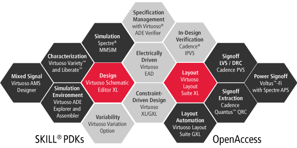
The Cadence custom and AMS flow includes the Virtuoso Analog Design Environment (ADE), Virtuoso Schematic Editor, Virtuoso Layout Suite with its Advanced-Node Platform, Virtuoso Space-Based Router, Spectre Circuit Simulator, Voltus-Fi Custom Power Integrity Solution, Quantus Extraction Solution, Physical Verification System, Litho Physical Analyzer, Cadence CMP Predictor and LDE Electrical Analyzer. These tools can be used throughout the complete custom AMS flow, including:

  • Front-end design: Corner, statistical, and reliability simulation; circuit and device checks; layout-dependent effect (LDE) analysis, and simulation and verification management.
  •  Custom layout design: An advanced, electro-migration and parasitic-aware environment that includes device and module generation, automated placement and routing, layout editing,  and dynamic DRC checking with Virtuoso Integrated PVS DRC, interactive PVS metal fill, in-design DFM flows for LDE, process hotspot repair (PHR), pattern analysis and optimization, and chemical mechanical polishing (CMP) check,  as well as support for correct-by-design multiple patterning flow.
  • Post-layout parasitic simulation and IR drop (IREM) analysis and integrated signoff: Including parasitic extraction, design rule checks, layout versus schematic checks, dummy metal fill and programmable electrical rule checks (PERC).
  • AMS design: Digital standard cell placement, pin optimization and automated space-based routing.


Filed Under: PCB design, Tools Tagged With: cadencedesignsystems, samsungelectronicsinc

Primary Sidebar

Featured Contributions

Design a circuit for ultra-low power sensor applications

Active baluns bridge the microwave and digital worlds

Managing design complexity and global collaboration with IP-centric design

PCB design best practices for ECAD/MCAD collaboration

Open RAN networks pass the time

More Featured Contributions

EE TECH TOOLBOX

“ee
Tech Toolbox: Internet of Things
Explore practical strategies for minimizing attack surfaces, managing memory efficiently, and securing firmware. Download now to ensure your IoT implementations remain secure, efficient, and future-ready.

EE LEARNING CENTER

EE Learning Center
“analog
EXPAND YOUR KNOWLEDGE AND STAY CONNECTED
Get the latest info on technologies, tools and strategies for EE professionals.

EE ENGINEERING TRAINING DAYS

engineering

RSS Current EDABoard.com discussions

  • Hard wired security cameras
  • Calculating inductor value for buck converter using XL1509 IC
  • i need an embedded c program that will read a 12 bit memory address from the io pins and output the data to pins from the memory in a 8051 mcontroller
  • Spice model for diode for rectifier simulation
  • Can I Flip Primary Connections on Mini-Circuits TCN1-10+ to Invert Output Polarity?

RSS Current Electro-Tech-Online.com Discussions

  • 12v battery, 18v magic
  • Back to the old BASIC days
  • Need help in repairing a dead motherboard
  • LED circuit for 1/6 scale diorama
  • how to work on pcbs that are thick
“bills

Design Fast

Component Selection Made Simple.

Try it Today
design fast globle

Footer

Analog IC Tips

EE WORLD ONLINE NETWORK

  • 5G Technology World
  • EE World Online
  • Engineers Garage
  • Battery Power Tips
  • Connector Tips
  • DesignFast
  • EDA Board Forums
  • Electro Tech Online Forums
  • EV Engineering
  • Microcontroller Tips
  • Power Electronic Tips
  • Sensor Tips
  • Test and Measurement Tips

ANALOG IC TIPS

  • Subscribe to our newsletter
  • Advertise with us
  • Contact us
  • About us

Copyright © 2025 · WTWH Media LLC and its licensors. All rights reserved.
The material on this site may not be reproduced, distributed, transmitted, cached or otherwise used, except with the prior written permission of WTWH Media.

Privacy Policy