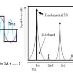
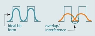
Digital signals representing data symbols may be presumed to be clean, consistent representations of ones and zeroes when they are launched onto their communications medium, whether it is a wired, wireless RF, or optical fiber link. However, due to bandwidth limitations of the medium, external and internal noise, crosstalk, multipath, reflections, and many other unavoidable imperfections, the signals are “smeared” in time, have timing jitter, and suffer amplitude variations. The symbols will even begin to spread (dispersion) and overlap with adjacent symbols representing other data bits, a situation called intersymbol interference (ISI), Figure 1.
Two very revealing techniques are used to assess the signal quality in real time and judge when and where to sample it to recover the original bits with the lowest bit error rate (BER). These are the eye diagram and the constellation diagram. Though they are separate perspectives on the quality and status of the received bit stream, together they are powerful tools for decided how to best re-capture those bits as well as observe the effect of adjustments to the receiver parameters.
Q: What is an eye diagram (sometimes called the eye pattern)?
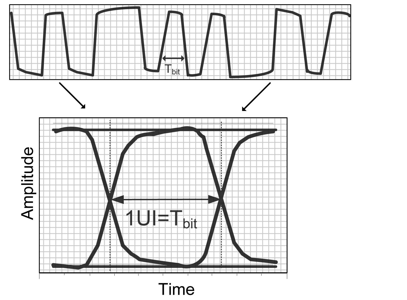
A: An eye pattern is created when all the bits of a received bit stream are overlaid on each other and an oscilloscope trace goes across the screen, Figure 2. The scope timing of this time-domain representation is set so that each bit begins another trace across the screen triggered by a system clock, and the screen is a little more than one-bit wide.
Q: What does “unit interval” mean in the context of eye diagrams?
A: The obvious way to specify the timing of a signal on the eye diagram is in terms of bit width, such as microseconds, nanoseconds, or femtoseconds. But this becomes a nuisance when the signal timing varies, as a function of the system clock, the data rate being used, and other factors, especially as some system adjust their data rate to meet bit error rate (BER) objectives.
Instead, eye-diagram discussion and analysis use the term “unit interval” (UI) which is a one-bit period but doesn’t define that period in terms of specific time value until the final part of the analysis. For example, a specification may state that the maximum jitter should be under 0.01 UI, and the RMS jitter should be below 0.005 UI, regardless of actual time period value of the UI.
Q: What does the eye diagram show?
A: The eye diagram is very revealing, Figure 3. At a glance, it qualitatively shows timing jitter, amplitude variations, noise effects, distortion, and more. It shows them in real time, so changes in the values of these factors due to circuit drift, noise variations, media changes, and more are easily observed.
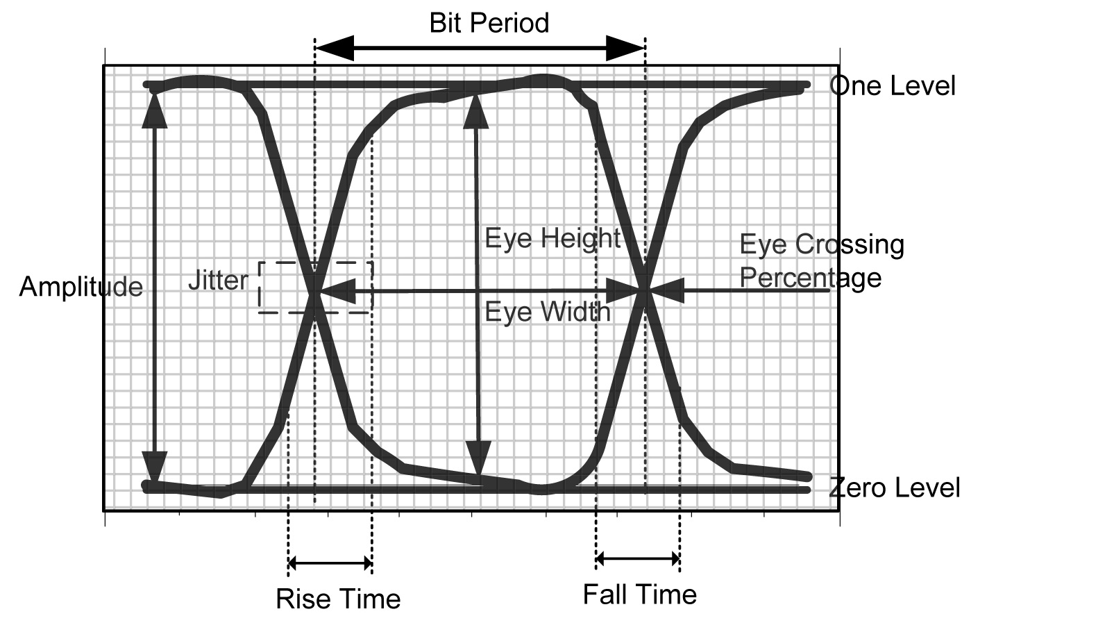
The eye diagram can also be used to quantitatively measure the received data bit “quality” to see if it meets standards for data recovery with low BER. It can even be used to dynamically guide adjustment of circuit parameters via hardware or software algorithms to improve performance as conditions vary.
Q: What does the term “eye opening” indicate?
A: It shows the amplitude between the upper and lower edges of the eye pattern., The opening has both maximum and minimum values, and in most applications, the minimum eye opening is the critical factors, as this shows the noise margin between the one and zero data-bit states. As the eye “closes,” it will be much more difficult to recover the data bits without error. Thus, one of the system-decoder objectives is to sample the signal when the eye opening is at its maximum. As system noise increases, the eye starts to close and so data recovery becomes more difficult.
Q: What about jitter?
A: Jitter, or minute variations in the recovered clock timing, also affects data recovery. It’s not enough to say the data should be sampled in the middle of the nominal unit interval, as jitter (and other distortions) may cause this “middle” to move. Ideally, if there were no jitter, the sampling could be set deterministically; instead, it may have to be adjusted dynamically to account for the jitter in the recovered bit stream.
Q: What else can the eye diagram show?
A: The eye diagram can also show if the data signal chain is symmetrical or if it is introducing offsets (DC bias) into the system. No system is perfectly balanced, and depending on the decoder/demodulator used, there will be an offset. This offset can affect the accuracy of the one/zero decoding, and many systems take extra steps to re-establish a zero-offset scenario if possible.
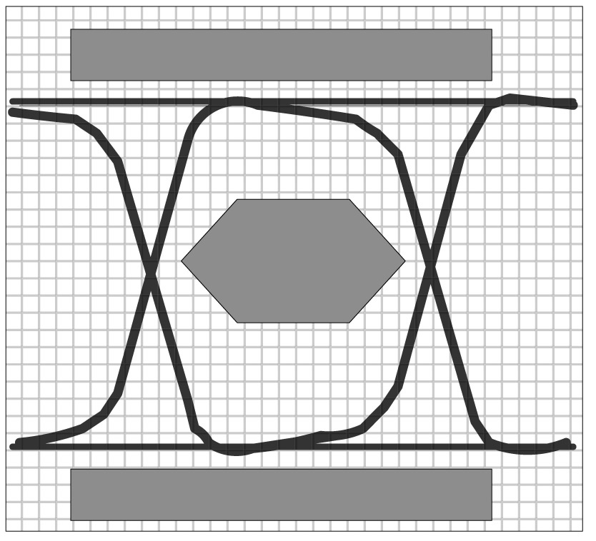
Q: What are some of the quantitative tools used in conjunction with the eye diagram?
A: Eye diagrams can be used for real-time assessment of signal quality versus industry or system standards using defined compliance masks, Figure 4. These are marked-off areas which show what is acceptable with respect to eye opening, timing jitter, and other factors to achieve satisfactory results. For example, the standard may say that the data recovery/decoding circuitry must deliver a certain level of performance, usually defined by BER, if the signal exceeds the mask-defined minimums. If the system cannot achieve this performance, adjustments need to be made to the hardware and software.
In summary, the eye diagram is a simple yet revealing time-domain display which shows jitter, amplitude, noise, and other characteristics both qualitatively and quantitatively. It is a dynamic display which also allows clear observation of system performance as external or internal conditions change or are deliberately varied.
Part 2 will look at constellation diagrams, which are another very useful visual indicator of recovered-signal performance. Although eye and constellation diagrams are not directly related, they are often used in conjunction for a comprehensive view of the data-channel performance.
References
- EE World Test & Measurement Tips, “The Eye Diagram”
- ON Semiconductor AND9075/D, “Understanding Data Eye Diagram Methodology for Analyzing High Speed Digital Signals”
- Keysight Technologies, “Using Eye Diagrams”