
A phase-lock(ed) loop (PLL) is a fundamental building block in wireless, radio frequency (RF), and telecommunication technologies. PLLs use a negative feedback circuit to match the phase of the frequency of another signal. PLLs synchronize the phase of the PLL’s output to the input signal’s frequency by tweaking the output of a voltage-driven oscillator; the PLL adjusts the oscillator to match what it sees at the PLL’s input. A feedback loop, or phase comparator, is used to compare the input signal with the output signal. PLLs are often used to duplicate or track the frequency of another signal. One use of a PLL is to synchronize the phase of a printed circuit board’s clock with an external signal.
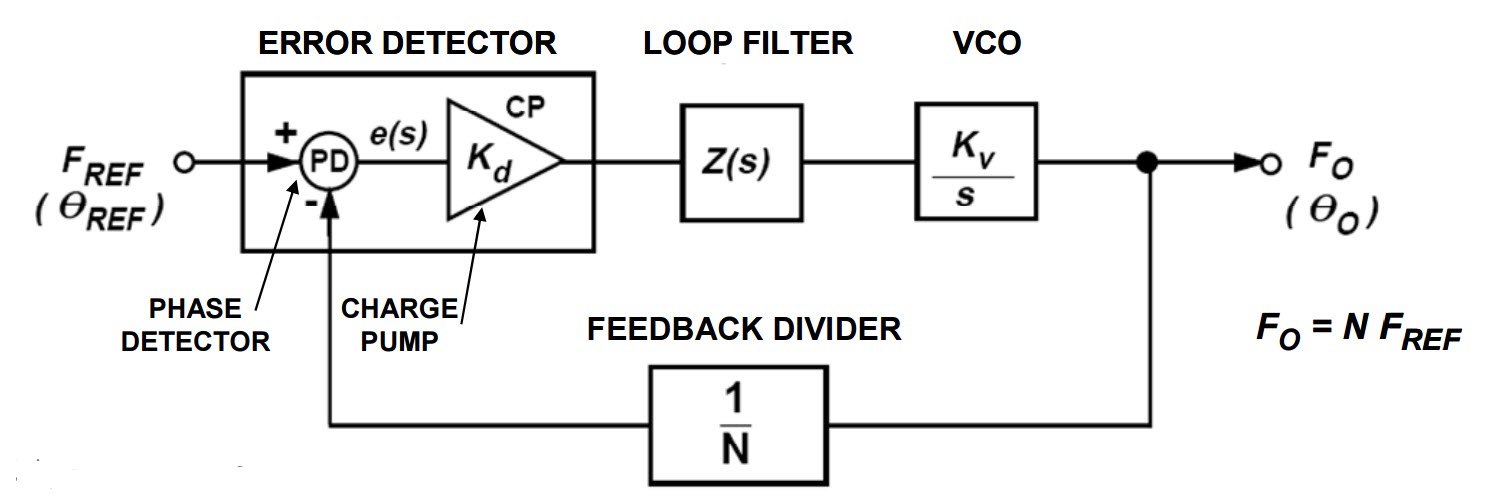
The above model of a PLL includes four basic elements.
1) A feedback divider with a variable N is called the N counter or the N divider. Since N is programmable in PLL integrated chips, the output can be in lock-step with the input or N can be adjusted so that the output is always a set amount out of phase with the input signal.
2) The error detector includes a phase-detector (PD) (which is also sometimes called a phase-frequency detector (PFD)), the node at which the reference frequency (input signal frequency, FREF) is compared with the feedback (output) signal. The charge pump is a source of current for the loop.
3) A Loop Filter, which is a low-pass filter (Zs) that controls the rate of change (frequency) of the voltage that goes to the VCO. The charge pump and the filter convert the digital output of the phase detector into an analog signal.
4) A voltage-controlled oscillator (VCO) offers the basis for oscillation in the circuit but is meant to be changed by feedback so that the output frequency (Fo) is a function of the reference frequency (FREF)and the adjustment of N.
Important parameters in the datasheet for a PLL are the operating frequency range or bandwidth of the application (measured in Hz), phase noise inherent in the PLL (measured in dB), an indicator of signal quality; and supply voltage. Applications for PLLs include clock distribution around a PCB (clock synthesis) and as sampling clocks for ADCs and DACs. Nearly all RF devices have a PLL since PLLs generate and modulate the carrier frequency in RF transmitters. RF receivers use PLLs to generate clock signals locally and to recover bit rate from noisy signals.
PLLs are used in cellular infrastructure, Wi-Fi, communications test equipment, microwave radios/backhaul, CATV equipment, satellite communications, optical modules, synchronous ethernet, broadcast video, wireless base stations, various military applications, and test and measurement.