• Skip to primary navigation
  • Skip to main content
  • Skip to primary sidebar
  • Skip to footer

Analog IC Tips

Analog IC Design, Products, Tools Layout

  • Products
    • Amplifiers
    • Clocks & Timing
    • Data Converters
    • EMI/RFI
    • Interface & Isolation
    • MEMS & Sensors
  • Applications
    • Audio
    • Automotive/Transportation
    • Industrial
    • IoT
    • Medical
    • Telecommunications
    • Wireless
  • Learn
    • eBooks / Tech Tips
    • FAQs
    • EE Learning Center
    • EE Training Days
    • Tech Toolboxes
    • Webinars & Digital Events
  • Resources
    • Design Guide Library
    • Digital Issues
    • Engineering Diversity & Inclusion
    • LEAP Awards
    • Podcasts
    • White Papers
    • DesignFast
  • Video
    • EE Videos
    • Teardown Videos
  • EE Forums
    • EDABoard.com
    • Electro-Tech-Online.com
  • Engineering Training Days
  • Advertise
  • Subscribe

Transient Voltage Suppressor Diode: What is it?

December 16, 2016 By Janet Heath

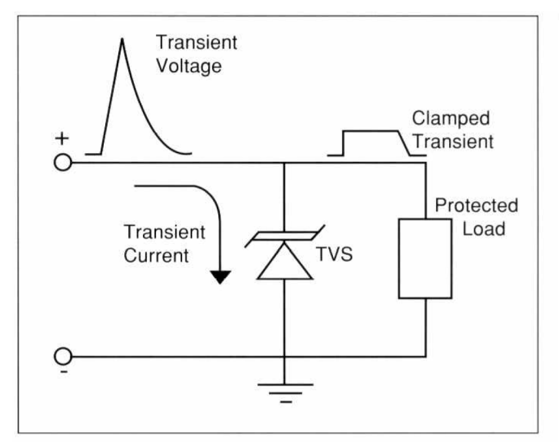
Transients are sudden high-frequency overvoltages that can destroy a chip. A silicon Transient Voltage Suppressor (TVS) is a circuit protection component that either attenuates (reduces) or filters a transient voltage spike (overvoltage), thus protecting your circuit. Another type of TVS diverts a voltage spike away from your circuit (also known as shunting, clamping, or bypassing.) TVSes protect circuits by utilizing the avalanche breakdown point of a silicon pn junction that’s created for this purpose. The pn junction returns to normal when the spike has passed and will clamp again on the next spike. In normal operation, the TVS is invisible to the circuit. A spike event that lasts a long time will necessitate the installation of a heat sink for the TVS, however. TVS devices are typically specified to handle in the range of kilowatts of peak power flowing through the TVS.

Figure 1: Voltage on the Y-axis exceeds the upper limit of 20V and is instantly clamped to an acceptable lever by the TVS in the circuit. TVSs respond rapidly. (Image: MicroSemi MicroNotes 103)

TVS diodes (and TVS diode arrays) protect circuits from Electrostatic Discharge (ESD). A TVS can protect a signal chain either unidirectionally or bi-directionally. A bidirectional TVS is chosen when the protected signal is usually supposed to swing above and below ground, as in an AC voltage or a DC signal intended to operate at positive and negative voltages. A unidirectional TVS diode will only allow voltage either above or below ground (positive or negative voltage.)

TVSes are often used to protect inputs. A USB receptacle or port is an ideal case since ESD is often experienced at the input of a device: when someone walks across a carpet to plug in a USB cable, a charge can build up that causes electrostatic discharge at that input. The TVS takes the jolt and immediately clamps it, or cuts it off, before the maximum voltage that the USB chip can withstand is reached.

Figure 2: A TVS is invisible to the circuit it protects. Here, it diverts the overvoltage on the input to ground. (Image: MicroSemi MicroNotes 103)

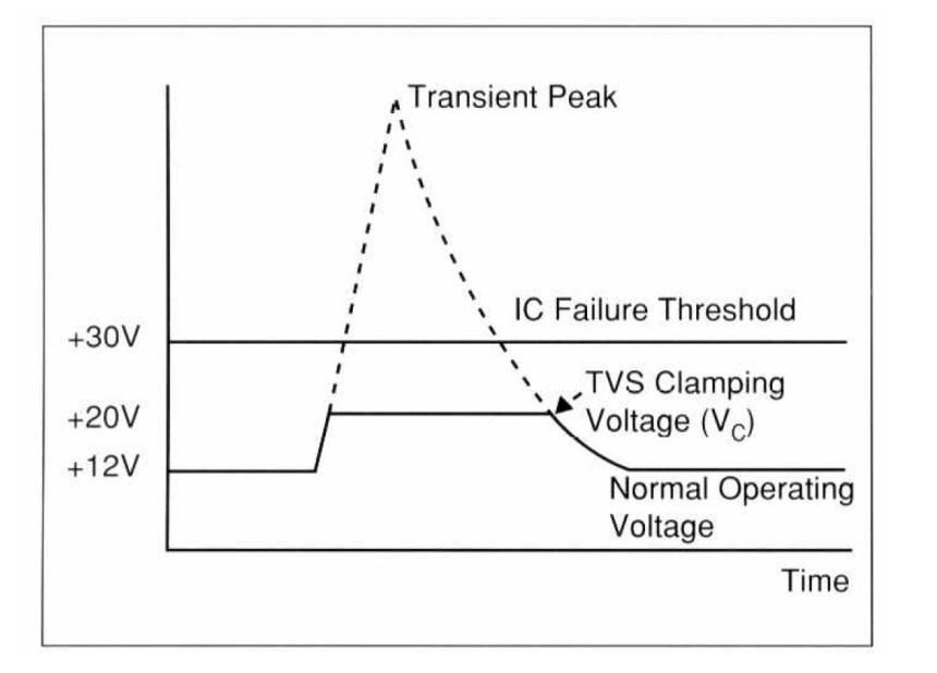
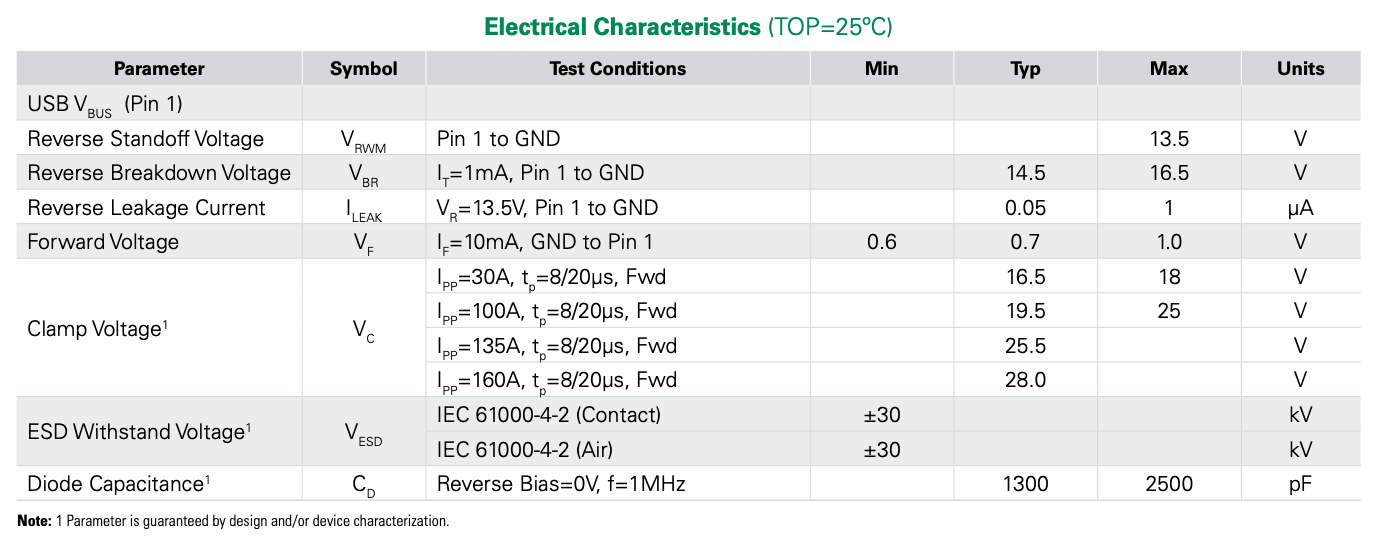
As for how to choose a TVS, make sure you know the maximum operating voltages for the devices in the protected circuit (load), as this will determine VWM, which is known in various datasheets as the working peak voltage, the maximum working voltage, the rated standoff voltage, reverse standoff voltage or maximum off-state voltage.  Littelfuse refers to VWM for a unidirectional TVS as “the maximum peak voltage that may be applied in the ‘blocking direction,’” if you expect to have no significant current flow. A bi-directional TVS is the same, except applies to both directions.[i] The VWM is typically 10 – 15% below the breakdown voltage (VBR). VBR is the voltage where TVS devices go into avalanche. Temperature affects VBR level, so VWM is at least 10% below VBR, as VBR may creep lower as temperatures drop. A TVS should not have a breakdown voltage equal to the working peak voltage.

The clamping voltage (VC) is the highest voltage that is specified in a TVS and is usually greater than VBR by 35 – 40% and ~60% higher than VWM. [ii] Peak pulse power (PPP) dissipation is another rating that factors into safely suppressing various transients or surges. Since:

PPP = VC x IPP,

where IPP is the worst-case surge current that is expected. The IEC 6100-4-2 standard describes measurement techniques and testing for certification that includes ESD protection and may be a valuable reference to help determine IPP.[iii] Other standards, such as the Human Body Model, may also be good references.[iv]

If there are still several TVSes to choose from, choose the TVS with the lowest capacitance value, especially when using them with high speed (high frequency) circuits.

Figure 3: Littelfuse’s SP1255 Series of TVS diode arrays protects the USB VBUs pin up to 160 amps. Capacitance and clamp voltages at varying currents are listed. (Image: Littelfuse SPA diode datasheet, SP1255 Series)

A TVS should also be physically placed near the input on the PCB.  Traces should be kept as short as possible to avoid parasitic capacitance.

Filed Under: Analog ICs, FAQ, Featured Tagged With: FAQ, littelfuse, microsemi

Primary Sidebar

Featured Contributions

Design a circuit for ultra-low power sensor applications

Active baluns bridge the microwave and digital worlds

Managing design complexity and global collaboration with IP-centric design

PCB design best practices for ECAD/MCAD collaboration

Open RAN networks pass the time

More Featured Contributions

EE TECH TOOLBOX

“ee
Tech Toolbox: Internet of Things
Explore practical strategies for minimizing attack surfaces, managing memory efficiently, and securing firmware. Download now to ensure your IoT implementations remain secure, efficient, and future-ready.

EE LEARNING CENTER

EE Learning Center
“analog
EXPAND YOUR KNOWLEDGE AND STAY CONNECTED
Get the latest info on technologies, tools and strategies for EE professionals.

EE ENGINEERING TRAINING DAYS

engineering

RSS Current EDABoard.com discussions

  • Hard wired security cameras
  • Calculating inductor value for buck converter using XL1509 IC
  • i need an embedded c program that will read a 12 bit memory address from the io pins and output the data to pins from the memory in a 8051 mcontroller
  • Spice model for diode for rectifier simulation
  • Can I Flip Primary Connections on Mini-Circuits TCN1-10+ to Invert Output Polarity?

RSS Current Electro-Tech-Online.com Discussions

  • 12v battery, 18v magic
  • Back to the old BASIC days
  • Need help in repairing a dead motherboard
  • LED circuit for 1/6 scale diorama
  • how to work on pcbs that are thick
“bills

Design Fast

Component Selection Made Simple.

Try it Today
design fast globle

Footer

Analog IC Tips

EE WORLD ONLINE NETWORK

  • 5G Technology World
  • EE World Online
  • Engineers Garage
  • Battery Power Tips
  • Connector Tips
  • DesignFast
  • EDA Board Forums
  • Electro Tech Online Forums
  • EV Engineering
  • Microcontroller Tips
  • Power Electronic Tips
  • Sensor Tips
  • Test and Measurement Tips

ANALOG IC TIPS

  • Subscribe to our newsletter
  • Advertise with us
  • Contact us
  • About us

Copyright © 2025 · WTWH Media LLC and its licensors. All rights reserved.
The material on this site may not be reproduced, distributed, transmitted, cached or otherwise used, except with the prior written permission of WTWH Media.

Privacy Policy