• Skip to primary navigation
  • Skip to main content
  • Skip to primary sidebar
  • Skip to footer

Analog IC Tips

Analog IC Design, Products, Tools Layout

  • Products
    • Amplifiers
    • Clocks & Timing
    • Data Converters
    • EMI/RFI
    • Interface & Isolation
    • MEMS & Sensors
  • Applications
    • Audio
    • Automotive/Transportation
    • Industrial
    • IoT
    • Medical
    • Telecommunications
    • Wireless
  • Learn
    • eBooks / Tech Tips
    • FAQs
    • EE Learning Center
    • EE Training Days
    • Tech Toolboxes
    • Webinars & Digital Events
  • Resources
    • Design Guide Library
    • Digital Issues
    • Engineering Diversity & Inclusion
    • LEAP Awards
    • Podcasts
    • White Papers
    • DesignFast
  • Video
    • EE Videos
    • Teardown Videos
  • EE Forums
    • EDABoard.com
    • Electro-Tech-Online.com
  • Engineering Training Days
  • Advertise
  • Subscribe

International Electron Devices Meeting to
look at novel ideas for analog circuits

September 28, 2015 By Lee Teschler

New semiconductor devices created with the Internet of Things in mind will be a hot topic at the 61st annual IEEE International Electron Devices Meeting (IEDM) taking place at the Washington D.C. Hilton Hotel from December 7-9, 2015. Considered a premier forum for scientists and engineers in the field of micro and nanoelectronics, IEDM this year includes several presentations oriented toward energy efficient devices catering to the needs of low-power electronics.

IGZO transistors
Scanning transmission electron microscope images showing views of the device in the channel length direction (left) and in the channel width direction (right).

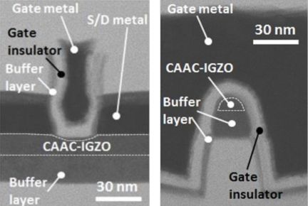
One such presentation covers high-frequency, low-leakage indium-gallium-zinc-oxide (IGZO) transistors. A team from Japan’s Semiconductor Energy Laboratory Co. will describe how they made 20-nm gate-all-around MOSFETs with super low off-state currents of < 0.1 pA, yet with cutoff frequencies exceeding 10 GHz. The transistors were made from thin films of IGZO. They were built using a self-aligned process that eliminated overlaps from the gate to the source and drain, rendering the channel immune from short-channel effects that otherwise would degrade performance. Integrated in a DRAM memory cell to demonstrate performance, their extremely low off-current allowed for data retention exceeding ten days at 125°C. The paper, 20-nm-node Trench-Gate-Self-Aligned Crystalline In-Ga-Zn-Oxide FET with High Frequency and Low Off-State Current; is by Daisuke Matsubayashi et al, Semiconductor Energy Laboratory Co., LTD.

InGaAs FETs
The photomicrograph at left is of a fin that has received five wet-HCL-based atomic-layer etch treatments to remove surface damage from previous process steps. The average roughness before and after the etching was measured to be only 0.5nm. The larger image at right is a transmission electron microscope view of a completed device, while the inset shows the gate stack.

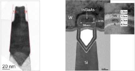
Another paper covers InGaAs nanowire FETs on silicon. Though III-V channels have benefits for low-power logic devices, there are have been questions about their manufacturability. At IEDM, a team led by Imec will discuss gate-all-around, high-performance InGaAs nanowire MOSFETs built on 300-mm silicon wafers. They have a high transconductance (gm = 2,200) that indicates despite having a lattice-mismatched substrate, the InGaAs channel material maintains its high carrier velocity. The paper, Gate-All-Around InGaAs Nanowire FETS with Peak Transconductance of 2200 μS/μm at 50nm Lg Using a Replacement Fin RMG Flow, is by N. Waldron et al, Imec/ASM.

Monolithic 3D chip
Top, a conceptual illustration of the device showing its heterogeneous functions; (center) the process steps needed to fabricate it; (bottom) a schematic of the CO2 far-infrared laser activation damage test on interconnect metallization (BEOL) and circuit functions (FEOL).

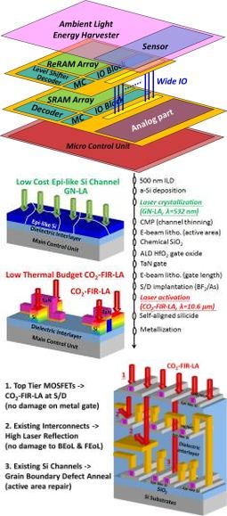
A point of emphasis at IEDM is that of integrating chip electronics and sensors on the same substrate to make IoT sensors that can be super-inexpensive. In that regard, a team led by Taiwan’s National Nano Device Laboratories investigated a way of improving the design of monolithic 3D chips. The normal way of constructing 3D circuits is by stacking separate chips and connecting them electrically with through-silicon vias (TSVs). But TSVs have significant disadvantages including relatively narrow I/O bandwidth. 3D ICs that are monolithic have no TSVs but their construction entails thermal annealing that can damage transistors — each layer in a 3D device must be annealed to remove stresses in its crystalline silicon structure, and also to activate the dopants which have been implanted in it.

The researchers addressed this issue by using a CO2 far-infrared laser at 400°C to selectively pulse-anneal specific areas of the silicon (the source-drain regions). They used this technique to build a sub-40-nm monolithic IC containing a variety of heterogeneous functions—logic, SRAM, RRAM, sense and analog amplifiers, and gas sensors. No device degradation was reported, and the researchers say their technique is suitable for making the low-power, low-cost, small-footprint and heterogeneously integrated devices needed for the Internet of Things.

The paper, Low-Cost and TSV-free Monolithic 3D-IC with Heterogeneous Integration of Logic, Memory and Sensor Analogy Circuitry for Internet of Things, is by Tsung-Ta Wu et al, National Nano Device Laboratories/National Tsing Hua University.

For registration and other information, visit the IEDM 2015 home page www.ieee-iedm.org, or contact Phyllis Mahoney, conference manager telephone (301) 527-0900 ext. 2.

Filed Under: Industry news

Primary Sidebar

Featured Contributions

Design a circuit for ultra-low power sensor applications

Active baluns bridge the microwave and digital worlds

Managing design complexity and global collaboration with IP-centric design

PCB design best practices for ECAD/MCAD collaboration

Open RAN networks pass the time

More Featured Contributions

EE TECH TOOLBOX

“ee
Tech Toolbox: Internet of Things
Explore practical strategies for minimizing attack surfaces, managing memory efficiently, and securing firmware. Download now to ensure your IoT implementations remain secure, efficient, and future-ready.

EE LEARNING CENTER

EE Learning Center
“analog
EXPAND YOUR KNOWLEDGE AND STAY CONNECTED
Get the latest info on technologies, tools and strategies for EE professionals.

EE ENGINEERING TRAINING DAYS

engineering

RSS Current EDABoard.com discussions

  • 12VAC to 12VDC 5A on 250ft 12AWG
  • Engineer's own PCB layout software guide?
  • Zeropole...
  • I think i have devised a new type of "super_transformer" for the Electricity grid?
  • Does mobility carrier ratio changes with Wn? (0.18um) inverter design

RSS Current Electro-Tech-Online.com Discussions

  • Lightbox circuit
  • I want to make a CRT with some modifications But i have no Idea where to start
  • Kawai KDP 80 Electronic Piano Dead
  • LT3511 Isolated Flyback Converter
  • Funny Images Thread!
“bills

Design Fast

Component Selection Made Simple.

Try it Today
design fast globle

Footer

Analog IC Tips

EE WORLD ONLINE NETWORK

  • 5G Technology World
  • EE World Online
  • Engineers Garage
  • Battery Power Tips
  • Connector Tips
  • DesignFast
  • EDA Board Forums
  • Electro Tech Online Forums
  • EV Engineering
  • Microcontroller Tips
  • Power Electronic Tips
  • Sensor Tips
  • Test and Measurement Tips

ANALOG IC TIPS

  • Subscribe to our newsletter
  • Advertise with us
  • Contact us
  • About us

Copyright © 2025 · WTWH Media LLC and its licensors. All rights reserved.
The material on this site may not be reproduced, distributed, transmitted, cached or otherwise used, except with the prior written permission of WTWH Media.

Privacy Policy