• Skip to primary navigation
  • Skip to main content
  • Skip to primary sidebar
  • Skip to footer

Analog IC Tips

Analog IC Design, Products, Tools Layout

  • Products
    • Amplifiers
    • Clocks & Timing
    • Data Converters
    • EMI/RFI
    • Interface & Isolation
    • MEMS & Sensors
  • Applications
    • Audio
    • Automotive/Transportation
    • Industrial
    • IoT
    • Medical
    • Telecommunications
    • Wireless
  • Learn
    • eBooks / Tech Tips
    • FAQs
    • EE Learning Center
    • EE Training Days
    • Tech Toolboxes
    • Webinars & Digital Events
  • Resources
    • Design Guide Library
    • Digital Issues
    • Engineering Diversity & Inclusion
    • LEAP Awards
    • Podcasts
    • White Papers
    • DesignFast
  • Video
    • EE Videos
    • Teardown Videos
  • EE Forums
    • EDABoard.com
    • Electro-Tech-Online.com
  • Engineering Training Days
  • Advertise
  • Subscribe

Open loop gain: how to measure with SPICE

November 14, 2013 By Chris Francis

When designing opamps in analog IC design, it is frequently required to plot the open loop gain/phase. One way of doing that is to use a high feedback resistor and very high capacitance so the feedback network has an extremely low corner frequency:

high feedback resistor

This works fine unless your opamp drive capability is low, in which case you can increase the feedback resistor. However, if the opamp also has a significant bias current that will shift the bias point of the opamp which could saturate the opamp output in extreme circumstances.

An improvement would be to add a unity gain voltage controlled voltage source (VCVS) in the feedback path to buffer the opamp output. The VCVS is the E source in SPICE:
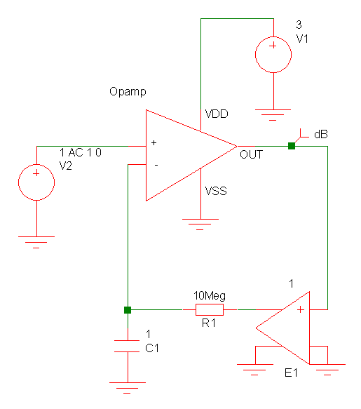
vcvs
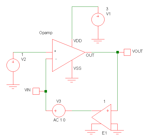
Another option is to use the VCVS but with no resistors or capacitors and derive the open loop transfer function from the ratio of output to input voltage as show below:

VCVS but with no resistors or capacitors

In this case the gain is VOUT/VIN. A comparison of the results of the three methods using an IC opamp with very limited output drive capability is shown below:

open loop gain

The results without the VCVS buffer show the effect of the limited opamp drive with a 10MΩ load. The results using the VCVS and the final method with no resistor/capacitor network are identical so the curves overlap.

An alternative is to use two VCVS sources to totally isolate the feedback. This can be useful if the opamp has a finite input bias current and the DC levels will be affected. An example is given below where the opamp on the left has a 10mV output offset due to the 10MΩ feedback resistance.two VCVS sources

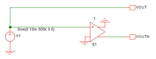
The VCVS has other uses such as if you want complementary signals. While this could be done with two separate voltage sources, if you want to alter the characteristics of one you then also have to edit the other. By connecting a VCVS with the output (or input) pins reversed you can have the two complementary signals – VOUT and VOUTN as shown below:

 

VOUT and VOUTN

You may also like:

  • noise simulation
    Demystifying SPICE noise simulation

  • What is an op amp?

Filed Under: Applications, FAQ, Industry Experts Tagged With: basics, FAQ, op amp, open loop, spice

Primary Sidebar

Featured Contributions

Design a circuit for ultra-low power sensor applications

Active baluns bridge the microwave and digital worlds

Managing design complexity and global collaboration with IP-centric design

PCB design best practices for ECAD/MCAD collaboration

Open RAN networks pass the time

More Featured Contributions

EE TECH TOOLBOX

“ee
Tech Toolbox: Internet of Things
Explore practical strategies for minimizing attack surfaces, managing memory efficiently, and securing firmware. Download now to ensure your IoT implementations remain secure, efficient, and future-ready.

EE LEARNING CENTER

EE Learning Center
“analog
EXPAND YOUR KNOWLEDGE AND STAY CONNECTED
Get the latest info on technologies, tools and strategies for EE professionals.

EE ENGINEERING TRAINING DAYS

engineering

RSS Current EDABoard.com discussions

  • 12VAC to 12VDC 5A on 250ft 12AWG
  • Engineer's own PCB layout software guide?
  • Zeropole...
  • Does mobility carrier ratio changes with Wn? (0.18um) inverter design
  • I think i have devised a new type of "super_transformer" for the Electricity grid?

RSS Current Electro-Tech-Online.com Discussions

  • Lightbox circuit
  • I want to make a CRT with some modifications But i have no Idea where to start
  • Kawai KDP 80 Electronic Piano Dead
  • LT3511 Isolated Flyback Converter
  • Funny Images Thread!
“bills

Design Fast

Component Selection Made Simple.

Try it Today
design fast globle

Footer

Analog IC Tips

EE WORLD ONLINE NETWORK

  • 5G Technology World
  • EE World Online
  • Engineers Garage
  • Battery Power Tips
  • Connector Tips
  • DesignFast
  • EDA Board Forums
  • Electro Tech Online Forums
  • EV Engineering
  • Microcontroller Tips
  • Power Electronic Tips
  • Sensor Tips
  • Test and Measurement Tips

ANALOG IC TIPS

  • Subscribe to our newsletter
  • Advertise with us
  • Contact us
  • About us

Copyright © 2025 · WTWH Media LLC and its licensors. All rights reserved.
The material on this site may not be reproduced, distributed, transmitted, cached or otherwise used, except with the prior written permission of WTWH Media.

Privacy Policy