
by Bill Schweber
Until fairly recently — roughly 15 to 20 years ago — sensors for ubiquitous physical parameters such as pressure, motion, and magnetic fields were relatively large, costly, power hungry, and electrically incompatible with standard circuitry. All that changed dramatically with the development of MEMS-based sensors (microelectromechanical systems) which etch a sensor into silicon by expanding on the well-developed fabrication processes and techniques already used for conventional electronic integrated circuits.
Beginning with the mass-market airbag sensor which quickly made the spring-loaded, ball-in-tube sensor obsolete and validated MEMS technology, these MEMS-based sensors have completely changed both how engineers think about sensing in general and, more importantly, what they can actually accomplish in their products. Products such as smart phones, drones, autonomous vehicles, and tactile feedback “fingers” now have one and often more tiny, low-cost, low-power accelerometers, gyroscopes, and other sensors on their crowded internal circuit boards, almost effortlessly providing high-performance sensing capabilities. Even microphones, which are acoustic-vibration transducers, have adopted MEMS technology for many situations including smartphones.
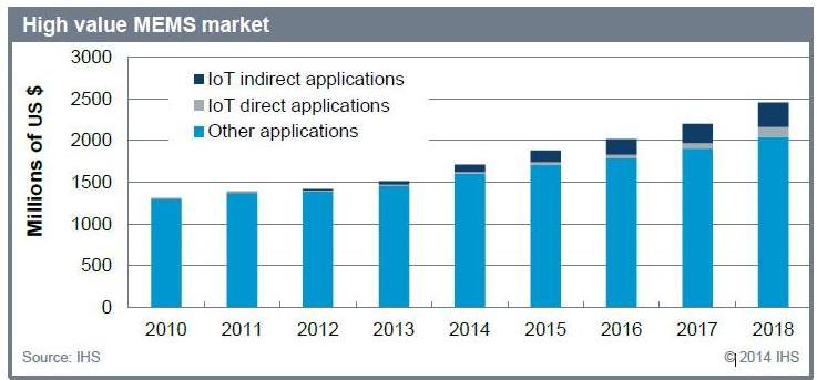
MEMS-based sensors for pressure, vibration, and location are also key enabling devices for the Internet of Things (IoT) as they make practical the long-term monitoring of key parameters in industry, commercial, and consumer/home environments. According to a December 2014 report “Internet of Things begins to impact High-Value MEMS” by specialist Jérémie Bouchaud from IHS Technology, “the worldwide market revenue for MEMS directly used in industrial IoT equipment will rise to $120 million in 2018, up from $16 million in 2013. In addition, MEMS will also be used to support the deployment of the IoT, such as devices employed in data centers. This indirect market for industrial IoT MEMS will increase to $214 million in 2018, up from $43 million in 2013,”
MEMS-based sensor applications span small, low-cost products to ones which are much larger and costlier. At one end, they are embedded in wearables to track use motion and pulse rates, while at the other end, today’s cars are loaded with multiple MEMS sensors to trigger airbags, sense impending rollover, adjust shock-absorber settings to match on load and road conditions, oversee brake performance, and monitor many other performance and safety-related factors.
Unlike their predecessor, larger “assembled” sensors which produced a simple, basic analog or crude digital output, MEMS devices have many outstanding virtues. They are:
- physically small (housed in low lead-count, surface-mount IC packages) and installed using standard production-line pick-and-place machines;
- very rugged, and can withstand shock of tens of thousands of g‘s if designed properly (think weapons and munitions);
- very low power, on the order of milliwatts, often operating from low-voltage supplies (down to 3 V in most cases, and even less), and compatible with energy-harvesting applications;
- suitable for monolithic multi-axis devices, such as an accelerometer for X, Y, and Z axes;
- available with processor-compatible I/O port (I2C or SPI) used for setting parameters and reporting results;
- often designed with calibration and compensation for non-linearities or temperature drift, as well as self-test;
- are able to evaluate their sensed signal versus user-set alarm thresholds, thus offloading the system processor.
MEMS sensors basics
Nearly all MEMS sensors use silicon, the most-common semiconductor material. However, unlike electronic circuits which use the element primarily for its electrical properties when it is “doped” to create a semiconductor, MEMS devices focus on its physical properties. It is an easily handled and etched crystalline material with consistent and rugged mechanical properties. It can simultaneously function as a mechanical and as an electronic component.
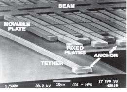
Consider the MEMS accelerometer, the first high-volume MEMS sensor and thus a major learning experience for both vendors and users. There are many ways to build this sensor: in one common approach, a “proof mass” with a side plate is etched into the silicon between fixed plates, and this mass is anchored by tethers acting as silicon springs on the side of its free-motion direction. Electrically, this structure is a micro-capacitor, with capacitance on the order of picofarads (one trillionth or 10−12 F) and even femtofarads (10−15 F), Figure 2a and Figure 2b.
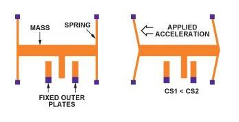
As the die accelerates along its active axis, the proof mass moves and the capacitance between the plates changes by a tiny amount, and this minute change is sensed and amplified by associated on-chip circuitry. After amplification, filtering, and buffering, the output corresponding to the proof mass’s displacement is available as an analog signal, or can be digitized within the MEMS device to provide a format compatible with the associated microcontroller.
Of course, this all sounds easy, but development of the first viable MEMS-based accelerometer was a long and difficult effort taking roughly a decade. Although it is based on well-known silicon-IC design and production techniques, those were developed for electronic circuit on silicon, not mechanical ones. Therefore, new design tools had to be developed which focused on modeling and production related to mechanical aspects (i.e. strength of materials, thermal issues), as well as the active circuitry.
Further, the standard silicon masking and etching techniques, which were mostly two-dimensional or had modest 3-D aspects, had to be greatly expanded to support complex masking and etching in a third dimension. This was necessary to allow for undercutting and allowing the proof mass to move. Packaging was also a challenge, as any minute particles which got trapped during the package cycle, or came from within the package itself, would interfere with motion of the proof mass. Standard electronic-production test systems and lines were also an issue, as they were designed to verify electronic performance. Now, however, there was a difficult mechanical aspect to the test as well, because the existing test systems for electromechanical-type sensors were not designed to handle IC packages.
Dramatic examples are evidence of change
While some sophisticated and quite successful systems were obviously built before MEMS devices became available, each sensing aspect was a challenge and major accomplishment. Many systems could only implement sensing along one or two dimensions due to cost, weight, power, and performance limits. A few MEMS-sensor examples show how this situation has changed; note that many MEMS sensors are related to motion and orientation, which are among the most difficult parameters to effectively sense, and yet are critical enablers for drones and IoT applications.
Acceleration: This includes basic acceleration, of course, as well tilt, shock, and vibration. Traditionally, this was measured for basic low-end go/no-go applications using mechanical devices such as a spring-loaded ball in a tube, or via a restricted pendulum and angle sensor. At the highest end, such as missile guidance, it is done using a PIGA (pendulous integrating gyroscopic accelerometer). Full three-axis acceleration requires three of these mounted in an orthogonal configuration. Some vibration applications, such as basic low-range vibrations sensors or microphones, use a different approach entirely, such as piezoelectric materials as their sensor. But this crystal functions only as a vibration-to-electrical transducer without signal conditioning or digitization, and thus requires additional circuitry to be useful.
Now, a small IC such as the ADXL343 three-axis digital accelerometer is an alternative, Figure 3. With user-selectable ranges of ±2, ±4, ±8, and ±16 g, this moderate-performance multipurpose accelerometer offers 10- to 13-bit resolution, with both SPI and I2C interfaces. It is housed in a tiny 3 mm × 5 mm × 1 mm LGA package, and can survive shock to 10,000 g (can the rest of the system even do that?). While performance of this devices is not as precise as a three-axis PIGA (although some other MEMS devices come amazingly close), the price is only a few dollars compared to hundreds of thousands of dollars per PIGA platform.
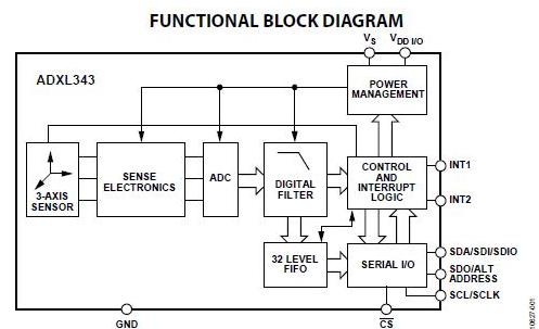
In addition to its basic performance capabilities, the ADXL343 includes internal logic to make basic motion-detection decisions. These include one-tap, double-tap, activity, inactivity, and free-fall detection, each with user-settable thresholds, and having the decisions in hardware within the MEMS IC dramatically offloads the system processor and its software. It operates from a 2.0 to 3.6 V rail, and power requirements can go as low as 23 μA, while its integral FIFO allows data to be buffered and then sent in a longer, power-saving stream.
Inertial measurement: A step above the triaxial accelerometer is a complete inertial measurement unit (IMU) which adds a gyroscope for assessing orientation in an absolute (inertial) frame of reference. This is needed where GPS is not available (underwater, indoors, or due to interference or spoofing), for implementing image stabilization, or if the system needs to cross-check the GPS results. Highest-performance IMUs use spinning-wheel gyros to stabilize the reference platform and are the extreme realization of mechanical and electronic design and implementation. These spherical units cost millions of dollars, consume hundreds of watts, range in size from about 10 cm to about 30 cm diameter, and weigh tens of kilograms.
In contrast, MEMS has made IMUs available to applications which cannot afford any of these specifications, admittedly with performance which, like that of the MEMS versus PIGA accelerometers, is not quite as good but certainly good enough for many applications. A six-axis IMU offers acceleration sensing along X, Y, and Z axes plus rotation sensing around those same axes, Figure 4.

For example, the LSM330DLCTR IMU from STMicroelectronics targets GPS-assisted car navigation, telematics, electronic tolling, and robotics, Figure 5. Basic specifications illustrate its performance capability: user-selectable full-scale acceleration range along each axis is ±2/±4/±8/±16 g, with full-scale rotation range around each axis of ±125/±245/±500/±1000/±2000 dps (degrees per second).
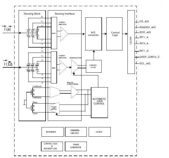
It is housed in a surface mount package which is only 4 × 5 × 1.1 mm high, operates from a 2.4 V to 3.6 V supply, and includes an SPI/I2C serial interface. Although its performance is not as good as a million-dollar gyro, all the other attributes (i.e. power, size, weight) are many orders of magnitude superior and sufficient for mass-market designs, thus enabling a wide range of IoT and autonomous vehicle/drone applications.
Conclusion
The impressive opportunities in mass applications such as the Internet of Things and autonomous/semiautonomous vehicles for land, water, and air are largely due to dramatic, nearly simultaneous developments across all aspects of technology. These include high-efficiency electric motors and controllers; lightweight, high-capacity batteries; tiny GPS receivers and processors; powerful central processors; effective RF links for control (whether smartphone or dedicated); and tiny high-resolution video cameras, among others.
Also critical have been the multiple sensors which have allowed remote guidance and navigation (with or without GPS), such as electronic compasses, and MEMS-based motion, acceleration, and inertial measurement units. In broad context, the availability of these high-performance devices has completely changed the design tradeoff balance, transforming sensors from large, costly, heavy, power-hungry transducers with incompatible electrical interfaces to their complete opposite.
About the Author:
Bill Schweber is an electronics engineer who has written three textbooks on electronic communications systems, as well as hundreds of technical articles, opinion columns, and product features. In past roles, he worked as a technical web-site manager for multiple topic-specific sites for EE Times, as well as both the Executive Editor and Analog Editor at EDN. He has an MSEE (Univ. of Mass) and BSEE (Columbia Univ.), is a Registered Professional Engineer, and holds an Advanced Class amateur radio license. Bill has also planned, written, and presented on-line courses on a variety of engineering topics, including MOSFET basics, ADC selection, and driving LEDs
(This article appears on Avnet.com, Sensing Solutions page along with related sensor content – Click here for more information