• Skip to primary navigation
  • Skip to main content
  • Skip to primary sidebar
  • Skip to footer

Analog IC Tips

Analog IC Design, Products, Tools Layout

  • Products
    • Amplifiers
    • Clocks & Timing
    • Data Converters
    • EMI/RFI
    • Interface & Isolation
    • MEMS & Sensors
  • Applications
    • Audio
    • Automotive/Transportation
    • Industrial
    • IoT
    • Medical
    • Telecommunications
    • Wireless
  • Learn
    • eBooks / Tech Tips
    • FAQs
    • EE Learning Center
    • EE Training Days
    • Tech Toolboxes
    • Webinars & Digital Events
  • Resources
    • Design Guide Library
    • Digital Issues
    • Engineering Diversity & Inclusion
    • LEAP Awards
    • Podcasts
    • White Papers
    • DesignFast
  • Video
    • EE Videos
    • Teardown Videos
  • EE Forums
    • EDABoard.com
    • Electro-Tech-Online.com
  • Engineering Training Days
  • Advertise
  • Subscribe

Miniature future for
passive electronic components

December 1, 2016 By Lee Teschler

Jürgen Geier, Christian Kasper, Jochen Neller, Bert Weiss
Rutronik

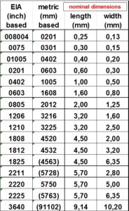
Passive electronic components are getting smaller, but the are also providing better performance within the same form factor. Twenty years ago form factors such as 1812 and 1206 were widely used. Today’s most commonly specified sizes are 0603 and 0402. The range extends down to 01005 (0.4 x 0.2 mm), and recently even to just 008004 (0.25 x 0.125 mm!).

table
MLCC dimensions
MLCC use
Data from Murata Manufacturing Co., Ltd. shows how the demand for smaller form factor MLCCs (Multi-Layer Ceramic Capacitors) is rising steadily.

The trend in SMD (surface mount device) resistors is also toward ever smaller form factors. Wired components are being replaced by this technology wherever possible. The 0201, 01005 and smaller form factors are used primarily in the mobile communications and tablet markets. Resistor networks – multiple resistors in one housing – also save space on the PCB. And high-power variants deliver twice the performance with the same housing form factor. Further miniaturization is taking place in the SMD current-measuring-resistor segment. New manufacturing technologies are enabling higher load capacities within the same form factor.

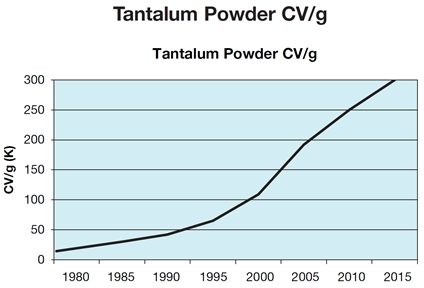
The form factors of tantalum capacitors – generally among the larger components – have diminished to such an extent over the last 20 years that they now take up only around 25% of the space they originally occupied on the PCB. Continual improvements in raw materials, smart component design and new manufacturing technologies have boosted volume efficiency in recent years.

tantalum-cap-data
Tantalum caps now take up only around 25% of the space they originally occupied on the PCB. Continual improvements in raw materials, smart component design and new manufacturing technologies have boosted volume efficiency.

Improvements in energy density of tantalum powder can only arise through continual development of powder grain size and properties. So the capacitance-to-voltage ratio per gram of tantalum powder (CV/g) is rising.

By optimizing the aluminum foil and the electrolyte used, for example, manufacturers can boost the capacitance while retaining the same form factor, while also extending service life many times over.

tantalum-powder
Data from AVX Corp. shows how the increasing energy density of tantalum powder is enabling miniaturization.

It should be noted also that such miniaturization does not necessarily lead to lower technical values in terms of ESR and ripple current. It is even possible to improve those values. So it is a good idea to keep a close watch on the latest developments in electrolytic capacitors because there are advances in the field happening regularly.

size-capacitance-comparison-one
Size/capacitance comparison based on two SMD series made by Panasonic Automotive & Industrial Systems. The FKS series has up to three times more capacitance compared to Panasonic FK series devices in the same can size. For example, a 25-V 33 µF FKS capacitor comes in a 4×5.8-mm can and uses just 62% of the space of previous generation parts.

size-capacitance-comparision-two

panasonic-inductors
Size/service life comparison based on three Panasonic SMD series inductors.

In the case of inductors, it might seem difficult to combine a high inductance with low dc resistance and small volume. Yet innovations such as improved multilayer and remolding technologies are making this possible today. A thin-film high-frequency inductor was recently launched featuring the ultra-miniature dimensions of 0.25 x 0.125 mm (008004), yet with the same quality grade Q as the larger form factor 01005 series.

quartz-crystals
Quartz crystals with smaller form factors do not necessarily require a new layout, as illustrated by this data from Murata Timing Devices.

Quartz dimensions of 3.2 x 2.5 mm are standard, though significantly smaller form factors such as 2.0 x 1.6 mm are already in wide use. Some manufacturers recommend accommodating 2016 sizes on 3225-size PCB pads. This does not necessarily mean the layout must be changed.

For quartz oscillators, MEMS technology and optimize chip design enable the quartz element and the resonant circuit to sit in ultra-miniature housings. As well as saving space, this combination also resolves accuracy and quality problems.

Real-time clocks (RTCs) in 3.2 x 2.5 x 1.0-mm packages are also available featuring extremely low current consumption. They are especially interesting for mobile, battery-powered applications.

Smaller components demand more precise and complex manufacturing techniques, in both fabrication and processing. A further aspect of the smallest form factors is that they are mostly more expensive than the larger sizes used in high volumes.

Below a certain size, the smallest form factors can no longer be replaced when in need of repair, and must be discarded along with the PCB. This can result in more production rejects and electronic scrap in the event of a fault.

Smaller – and so more densely packed – PCBs require more stringent protection against ESD, electromagnetic interference, and thermal problems. They often need more interference suppression components. At the same time, small form factors may help suppress interference because they can sit at the source of the interference or load site, reducing unwanted parasitics such as leakage inductance or stray capacitance.

Miniaturization also delivers lighter weight, less of a need for storage areas, and – not least – savings on raw materials. So the trend toward miniaturization is bound to continue.

Filed Under: Capacitors, Clocks & Timing, Inductors, Resistors Tagged With: rutronik

Primary Sidebar

Featured Contributions

Design a circuit for ultra-low power sensor applications

Active baluns bridge the microwave and digital worlds

Managing design complexity and global collaboration with IP-centric design

PCB design best practices for ECAD/MCAD collaboration

Open RAN networks pass the time

More Featured Contributions

EE TECH TOOLBOX

“ee
Tech Toolbox: Internet of Things
Explore practical strategies for minimizing attack surfaces, managing memory efficiently, and securing firmware. Download now to ensure your IoT implementations remain secure, efficient, and future-ready.

EE LEARNING CENTER

EE Learning Center
“analog
EXPAND YOUR KNOWLEDGE AND STAY CONNECTED
Get the latest info on technologies, tools and strategies for EE professionals.

EE ENGINEERING TRAINING DAYS

engineering

RSS Current EDABoard.com discussions

  • Hard wired security cameras
  • Calculating inductor value for buck converter using XL1509 IC
  • i need an embedded c program that will read a 12 bit memory address from the io pins and output the data to pins from the memory in a 8051 mcontroller
  • Spice model for diode for rectifier simulation
  • Can I Flip Primary Connections on Mini-Circuits TCN1-10+ to Invert Output Polarity?

RSS Current Electro-Tech-Online.com Discussions

  • 12v battery, 18v magic
  • Back to the old BASIC days
  • Need help in repairing a dead motherboard
  • LED circuit for 1/6 scale diorama
  • how to work on pcbs that are thick
“bills

Design Fast

Component Selection Made Simple.

Try it Today
design fast globle

Footer

Analog IC Tips

EE WORLD ONLINE NETWORK

  • 5G Technology World
  • EE World Online
  • Engineers Garage
  • Battery Power Tips
  • Connector Tips
  • DesignFast
  • EDA Board Forums
  • Electro Tech Online Forums
  • EV Engineering
  • Microcontroller Tips
  • Power Electronic Tips
  • Sensor Tips
  • Test and Measurement Tips

ANALOG IC TIPS

  • Subscribe to our newsletter
  • Advertise with us
  • Contact us
  • About us

Copyright © 2025 · WTWH Media LLC and its licensors. All rights reserved.
The material on this site may not be reproduced, distributed, transmitted, cached or otherwise used, except with the prior written permission of WTWH Media.

Privacy Policy