• Skip to primary navigation
  • Skip to main content
  • Skip to primary sidebar
  • Skip to footer

Analog IC Tips

Analog IC Design, Products, Tools Layout

  • Products
    • Amplifiers
    • Clocks & Timing
    • Data Converters
    • Interface & Isolation
    • MEMS & Sensors
  • Applications
  • Video
    • TI Video Channel
  • EE Forums
    • EDABoard.com
    • Electro-Tech-Online.com
  • EE Resources
    • DesignFast
    • eBooks / Tech Tips
    • FAQs
    • LEAP Awards
    • Podcasts
    • Webinars
    • White Papers
  • EE Learning Center

One chip, multiple LTE signals for 3G, 4G, and 5G macro cell TDD base station work

August 24, 2018 By Lee Teschler

Matt Purvis from ADI recently took us through a demo of a super-wideband RF transceiver chip that targets the expanding 5G telecom area. The point of the chip is to transmit multi-carrier LTE signals and to simplify the task of designing MIMO systems. Called the ADRV9009, it is a single-chip time division duplex (TDD) design primarily aimed at time-domain switching. So it has features that handle switching the transmitters and receivers on and off. It also handles fast frequency hopping down to a 60 μsec dwell time for each hop, and the radio maintains calibration across those hops. The chip contains two transmitters, two receivers and two observation receivers for loopback calibrations. And there’s a 200 MHz bandwidth on the receiver and the transmitter.

ADRV9009
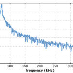
During the demo, Purvis displayed the chip outputs on a spectrum analyzer for us. We were able to see a five-carrier LTE signal with the analyzer set for a 250 MHz span. That gave us a good view of five 20-MHz LTE signals, all coming out of a single chip.

Purvis also showed us an evaluation platform at RadioVerse for the ADRV9009. It includes access to the two transmitters, two receivers, and two observation receivers for calibration and then, additionally, an external LL for more stringent baseband requirements.

You may also like:

  • electrical noise
    Electrical noise, Part 1: Introductory concepts
  • active noise cancellation
    Active noise cancellation, Part 2: Implementation
  • load pull
    Load pull for RF devices, Part 1: What and why

  • Radio receiver architectures, Part 1—TRF and Superhet

Filed Under: Applications, Featured, Telecommunications Tagged With: analogdevices

Primary Sidebar

Subscribe to Our Newsletter

Subscribe to weekly industry news, new product innovations and more.

Subscribe today

EE Training Center Classrooms

“ee

“ee

“ee

“ee

RSS Current EDABoard.com discussions

  • Why do some op amps have a higher GBW than what the unity gain-bandwidth is?
  • I need to transform a c code archive into a .hex archive. (Desperatly)
  • Modeling Issues with Aperture Coupled slot antenna
  • how to connect 32 push buttons to atemga328p?
  • Will this RF power transistor work for RF power amp at 2.4 GHz?

RSS Current Electro-Tech-Online.com Discussions

  • This part is driving me nuts .....
  • Any advice on identifying the HV wires on an old flyback.
  • How do I find the value of an exploded ceramic capacitor?
  • Jon's Imaginarium - Microchip FilterLab Program and Graph Paper Printer Program by Dr. Philippe Marquis
  • Test

Follow us on Twitter

Tweets by AnalogICTips

Design Fast

Component Selection Made Simple.

Try it Today
design fast globle

Footer

Analog IC Tips

EE WORLD ONLINE NETWORK

  • EE World Online
  • EDA Board Forums
  • Electro Tech Online Forums
  • DesignFast
  • Connector Tips
  • Microcontroller Tips
  • Power Electronic Tips
  • Sensor Tips
  • Test and Measurement Tips
  • Wire and Cable Tips
  • 5G Technology World

ANALOG IC TIPS

  • Subscribe to our newsletter
  • Advertise with us
  • Contact us
  • About us
Follow us on Twitter Add us on Facebook Follow us on YouTube Follow us on Instagram

Copyright © 2021 · WTWH Media LLC and its licensors. All rights reserved.
The material on this site may not be reproduced, distributed, transmitted, cached or otherwise used, except with the prior written permission of WTWH Media.

Privacy Policy