
I was recently thinking about the issues surrounding rail to rail input opamps and the problems of making them low distortion – a problem I have had to overcome when designing integrated circuits for instrumentation applications. Some rail to rail opamps use two input stages – one using NMOS input transistors, the other using PMOS and then combine the two. So, near the negative rail, the PMOS input stage is used and the NMOS one stops working. Near the positive rail, the opposite happens. In between, you end up with a combination of the two input stages contributing to the output voltage (or current). This is probably best illustrated with an example. A simplified conventional PMOS input stage might look something like this (ignore transistor dimensions).
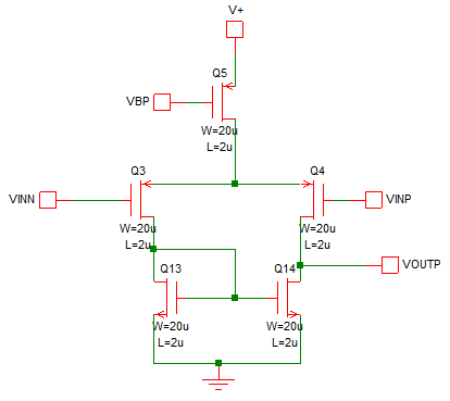
Q3 and Q4 are your input transistors and the current mirror Q13/Q14 produces your output. Depending on transistor sizing you will be able to make the circuit work down to the negative supply rail and even slightly below but it will not work near the positive supply rail.
Adding an NMOS input stage gives two pairs of outputs which then need to be combined to produce the final output.
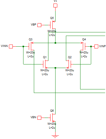
Here Q1 & Q2 are the NMOS input transistors. The two sets of outputs need combining to produce a final, single output. One of the problems with this rail-to-rail technique is that the open loop gain and bandwidth will change depending on the input voltage as you change from the NMOS inputs operating, to both NMOS and PMOS inputs operating, to only PMOS, although there are various techniques to try to improve the resulting imbalance.
A long time ago I read a paper in the IEEE Journal of Solid State Circuits discussing various solutions to the problem including using a charge pump to produce a higher voltage to drive the input stage current source, so a PMOS input stage can cover the rail to rail input without the need for the NMOS input stage. So it was interesting to recently come across the Texas Instruments OPA388 which uses the voltage pump technique to produce a low distortion rail to rail opamp which is also chopper stabilized, so it has very low offset with no 1/f noise. Texas Instruments describe some of their techniques in their TechNotes SBOA181A and SBOA182A which are worth reading in conjunction with the OPA388 datasheet. This image from SBOA181A shows the simplified input stage with the charge pump.
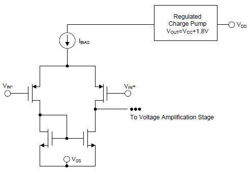
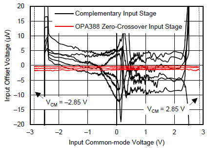
It is simply a conventional PMOS input stage with a charge pumped current source supply. The real circuit will be a lot more complex. They also show a couple of plots to illustrate the effect of the zero crossover circuitry compared to “conventional” complementary rail to rail input stages.
When you consider the 5µV maximum offset, 10MHz unity gain bandwidth, low distortion, and rail-to-rail input and output, it all seems pretty good. It does claim to be low noise and certainly, if you look at the 0.1Hz to 10Hz noise at 0.14µV peak to peak, it is low noise. However, the mid-band noise is 7nV/rt(Hz) which isn’t really that low, but then you have to consider it in the context of the other parameters. You can find an opamp with high input impedance with lower mid-band noise but probably not with the low offset or rail to rail inputs. As with most choices you can have some combination of parameters from your ideal wish list but not usually all of them. You pick the ones that are most important to you and balance one parameter against another. With noise, you need to look at the frequency band you are working over and calculate total noise, taking into account both mid band and 1/f noise.
OPA388 PSPICE and TINI-TI models are available on Texas Instruments’ web site.