Part 2 of this article continued the exploration of the basic optical tweezer. This part builds up to a complete system, DIY optical tweezer systems, and extensions to the basic optical-tweezer arrangement.
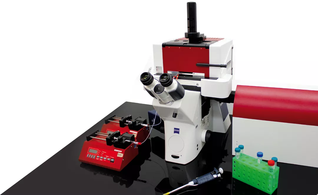
The optical tweezer is obviously not a simple system, and a complete system requires lenses, dichroic mirrors, a laser, video camera, isolation against vibration, and more (Figure 1). If all this seems somewhat mystical, magical, and perhaps even unbelievable – well, this is quantum physics, so that’s a very normal reaction. Nonetheless, every part needed can be purchased as standard component.
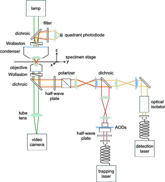
The detailed construction of an optical tweezer is unlike most instrumentation related to tiny particles and even particle physics, where you need ever-larger and more-costly equipment as the particles get smaller (think of supercolliders). You can buy the basic parts to build a tweezer (laser, special lenses, beam-steering mirror, dielectric mirror, and camera) for a few thousand dollars and make one yourself—and student labs have done this. Most DIY designs being with a standard optical microscope, but some instead also include the construction of the optical microscope but only with the lenses and features needed for the optical tweezes and leave out any unnecessary features of a general-purpose microscope (Figure 2).

Though developed by physicists, optical tweezers have become essential tools in biology, medicine, and chemistry for manipulation of tiny objects from test spheres to DNA strings (Figure 3).
Of course, commercial optical tweezers are now readily available. A typical unit is available from Bruker Corp, and it is offered with an option which adds an atomic force microscope (AF) to the basic optical tweezer (Figure 4), a function and instrument needed for precise sample assessment and mapping.
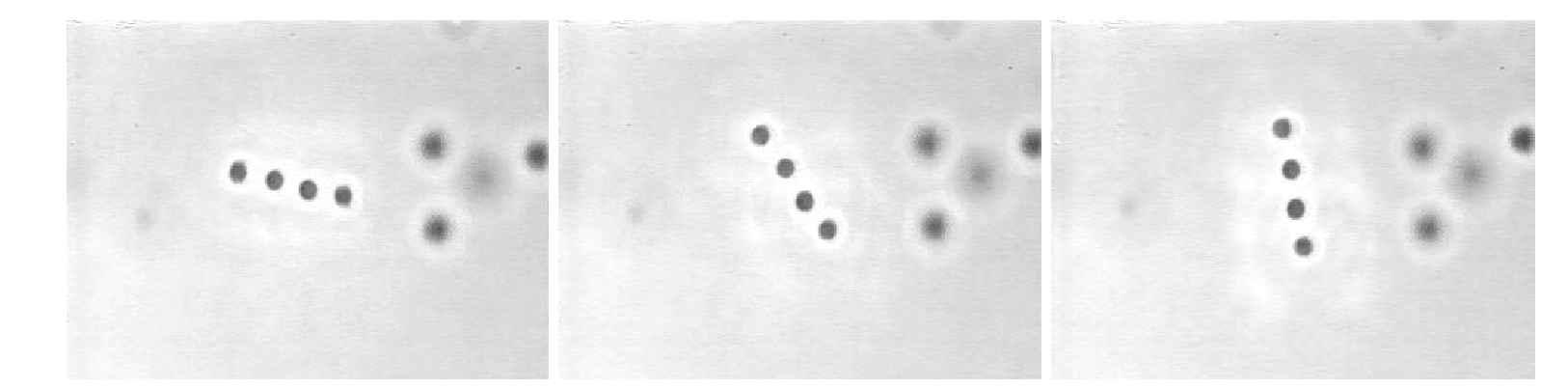
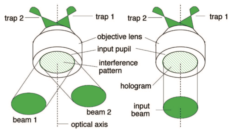
As expected, there have been numerous improvements and enhancements in performance, functionality, size, and cost since the earliest days of the optical tweezer, driven by advances in lasers, closed-loop computer control, data analysis. piezoelectric positioning, and precision motors, to cite just a few areas. Some designs even provide multiple traps to create microfluidics devices that can be used for cell sorting and biomedical diagnostics (Figure 5).
Conclusion
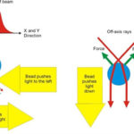
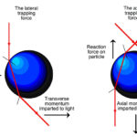
Innovation often comes from unforeseeable sources and combinations of factors. For the optical tweezer, it was the development of the laser, use of conical lenses for shaping the laser output into Bessel beams, deep insight into the basic physics from two perspectives, and the need to handle and manipulate tiny particles and strands. This sort of advance, like magnetic resonance imaging, would not have been envisioned by the many predictions of progress via simple extrapolation, such as the well-known semiconductor “road map” and Moore’s Law which has defined ICs for the past decades, with their emphasis on continuous feature-shrink cycles along with increased transistor density.
EE World References
Assembling Micro-Components With Laser Tweezers
Nanotweezer Is New Tool To Create Advanced Plasmonic Technologies
A Levitated Nanosphere As An Ultra-Sensitive Sensor
The difference between scanning electron microscopes and tunneling scanning electron microscopes
The instrumentation of nanotechnology
Magnetic resonance imaging (MRI), Part 1: How it works
MRI, Part 2: Historical development (and lawsuits)
Nanowires As Sensors In New Type Of Atomic Force Microscope
Atomic Force Microscope Reveals Chemical Ghosts
External References
- Ashkin, A., “Acceleration and Trapping of Particles by Radiation Pressure,” Physical Review Letters, 1970. 24(4): p. 156
- Justin E. Molloy and Miles J. Padgett, “Lights, action: optical tweezers,” (Contemporary Physics), 2002, volume 43, number 4, pages 241 to 258.
- Trygve Bakken & Adam Koerner, “Optical Tweezers,” University of California at San Diego, Biophysics Lab, June 2009.
- “Optical trapping: How does it work?, University of St. Andrews, Scotland.
- Stanford University, “An introduction to optical tweezers”
- Arvix.org (Cornell University), “Step-by-step Guide to the Realisation of Advanced Optical Tweezers”
- Harvard University, “Inexpensive optical tweezers for undergraduate laboratories”
- Review of Scientific Instruments, “Optical Trapping” (via Semantic Scholar)
- Wikipedia, “Bessel beam”