Despite appearances, there’s nothing simple about the materials or fabrication of the ubiquitous PC board, and the requirements of multi-GHz systems are increasing the performance demands placed on these boards.
We take the standard, usually green, printed circuit board (PC board or PCB) for granted, but it has an interesting history, alternatives, and future. This FAQ will explore various aspects of this literal and figurative foundation of modern electronic circuitry and systems. Despite their simple appearance, printed circuit boards are highly engineered, sophisticated passive components, and getting even more so with the growth of multi-GHz designs such as 5G (but not limited to that application).
(Note that some industry organizations tried to change the phrase “PC board” to the perhaps more-descriptive “printed wiring board” — thus, PW board, or PWB — but this didn’t catch on; the printed “circuit” name seems to have stuck.
Q: What is a PC board?
A: It’s a laminated combination of an insulating substrate with a conductive copper cladding on one or both sides. It can be made different materials (more on this later) which act as the mechanical base for the resultant copper tracks (traces) which are the interconnections between the various circuit components.
Q: Is it really “printed”?
A: No, it is not, although there have been research efforts (and there still are) to actually print the circuitry with conductive inks just as a book is printed on a printing press. It is not a technique in wide use at this time; it is viable only in specialty applications.
Q: How is the copper’s desired trace pattern established?
A: There are two ways. In the most common technique, the desired areas are covered with a mask material which acts as a resist to acid, and then the undesired copper is chemically etched away using that acid. The less-used alternative is additive deposition where copper is electroplated in the desired areas. The choice is based on cost, board size, trace width, mechanical and physical tolerances, and many other factors
Q: Before we get further into the present PC board, what is the background of the concept?
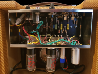
A: Prior to the late 1950s and 1960s, when “electronics” was largely a world of higher voltages and vacuum tubes, circuits were hand-wired. Various sockets and terminal strips were attached to a baseboard or plate of metal, Bakelite (a plastic made from synthetic components; it is thermosetting phenol-formaldehyde resin, formed from a condensation reaction of phenol with formaldehyde), wood, or wood chips pressed in resin. Other components such as resistors or capacitors were soldered to the terminal strips, and the interconnections were made with individual wires which were soldered to the various connection points (Figure 1). Layout and dressing of the wires were important aspects of a clean, producible product that could also be repaired in the factory or field.
Q: Sounds laborious, did it work?
A: Yes, it did: millions of consumer, industrial, and mil/aero products were built this way, and successfully used for decades.
Q: What happened?
A: In a word: solid-state devices. Discrete diodes, transistors, and then integrated circuits were developed and improved, and they were physically incompatible with this sort of mounting and interconnection. Transistors and diodes with their thin wire leads and single/dual in-line packaged ICs (SIPs and DIPs) could not be attached or soldered in this way. Sockets could be used for some of the components, but the arrangement was awkward, costly, space-consuming, and not reliable. Some systems used standard-size modules with interconnects at specific points, but this will be costly and inflexible.
Q: What were the first PC boards like?
A: The first circuit boards, in the 1960s, were made of pressed paper and phenolic resin and had a tan color (Figure 2). They were clad with copper on one side only, and the unwanted copper was etched away. The traces were relatively wide – 2-3 millimeters at a minimum, typically – and their spacing was on the same order.
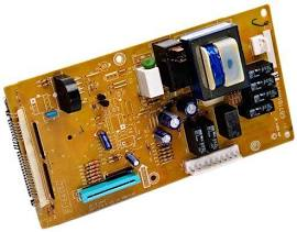
The holes needed for mounting components were punched (not drilled) and then components were inserted and soldered. These steps were initially done by hand and soon upgraded to machine insertion and wave-soldering machines. These phenolic boards eventually received an industry designation as FR-2 (FR means “fire-resistant).
Q: Are these single-sided boards obsolete?
A: Actually, no. They are still used in some mass-market applications, primarily appliances such as microwave ovens or coffee machines, where the electronics are simple and there are also larger power devices (MOSFETs, for example). Phenolic is inexpensive, punching holes is quick and cheap, and the boards are a good match for the application. In these layouts, designers use wire jumpers or even zero-ohm resistors (a standard catalog item) to create a layout which needs wiring (the traces) on one side only.
Q: Are their standards for PC boards? Who sets them?
A: Absolutely yes. These standards allow a PC-board user to go to several vendors with requirements and get comparable estimates. They also allow the PC board fabricators to use consistent systems to take orders, model and build system which work consistently with boards from different sources and for different users. Other standards are related to safety, flammability, and electrical and mechanical parameters performance. There are also microwave-spectrum standards which are increasingly important (more on this later).
In addition to industrial-focused NEMA standards, the primary standards-setting organization is the IPC, a global trade association for the printed-board and electronics-assembly industries, their customers and suppliers. IPC was founded in 1957 as the Institute for Printed Circuits, then changed its name to Institute for Interconnecting and Packaging Electronic Circuits, and then changed it to the more-anonymous IPC (just letters, no words).
Part 2 of this FAQ looks at the ubiquitous FR-4 PC board as well as other PC board issues.
References
- Wikipedia, “FR-4”
- PCB trace calculators: MustCalculate, Bittele Electronics Inc. and Trance-Cat
- Wikipedia, “Printed circuit board”
- Wikipedia, “Via (electronics)”
- SEEED Studio, “Printed Circuit Board(PCB) Material Types and Comparison”
- Al Wright, Epec LLC., “PCB Vias – Everything You Need To Know”
- Microwaves101, “FR-4”
- All About Circuits, “Which Via Should I Choose? A Guide to Vias in PCB Design”
- Rogers Corp., “Evaluating PCB Plated Through Holes For 5G Applications”
- John W. Schultz, Compass Technology Group, “A New Dielectric Analyzer for Rapid Measurement of Microwave Substrates up to 6 GHz”
- Rogers Corp., “Characterizing Circuit Materials at mmWave Frequencies”
- Rogers Corp., “Laminate Materials Simultaneously Increase μ and ε, Reducing Antenna Size”
Related EE World Content
- What are RF waveguides? Part 1: context and principles
- What are RF waveguides? Part 2: implementation and components
- Passive microwave components, Part 2: couplers and splitters
- Passive microwave components, Part 1: isolators and circulators
- Next-gen laminates improve insertion loss in automotive radar sensor applications
- High-impedance laminates help reduce antenna size
- Laminates for 5G and other millimeter wave applications