Part 1 of this FAQ series looked at the ubiquitous FR-4 PC board as well as other PC board issues, and Part 2 reviewed highlighted some of the board issues and the widely used FR-4 PC board substrate. This third part looks at advanced PB board issues such as vias and multilayer boards.
Q: How is a basic FR-4 PC board priced?
A: Obviously, it depends on many factors: board size and shape (it does not have to be rectangular), substrate thickness, cladding thickness and type (single or double-sided), how fine the trace lines are, and the allowable tolerances, among other factors. It also depends on the number and size of the holes to be drilled. In fact, many PC board fabricators do their first BOM estimate solely using board type (substrate and cladding thicknesses), size, and the number of holes.
The industry adoption of surface mount technology (SMT) components in the 1990s in place of through-hole components dramatically cut the size of many boards as well the number of holes required (which could easily reach into the hundreds and even thousands) and thus the cost – both unintended benefits. However, board density increased while tolerances became tighter, both of which increased the cost, in an ironic sort of “payback.”
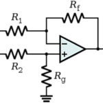
Q: What can be done if the board is large and flexes to excess?
A: Obviously, a thicker substrate can be used, but this may be inadequate and costly in terms of materials and drilling time. An alternative is to use a bus bar which inherently also functions as a stiffener, Figure 1.
The bus bar is a standard, low-cost, easy-to-use component which carries DC power across the board on a separate raised path (a two-layer bus bar can also act as ground-current return), and is primarily used to reduce IR drop and thus also I2R dissipation. It has the useful additional benefit of stiffening the board and also enables PC board trace layouts with shorter signal paths and improved signal integrity.
Q: What if a two-layer PC board cannot handle the complexity of the circuit, or provide enough power and ground paths?
A: By the 1990s, PC board technology achieved sufficient precision and consistency that multiplayer boards became practical. This arrangement uses a “stack-up” of a series of single-layer boards, with the top (or bottom) board having two layers in most cases, so both the visible top and bottom of the multilayer stackup are available for components. Typically, in a four-layer PC board, the top and bottom cladding layers are used for signals, with SMT components mounted on those layers, while one inner layer is used for power and the other is used for return-current path as well as signal common. The inner layers, with their large amounts of surface copper, are also used for heat sinks, to draw dissipated heat away from components.
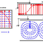
Q: How do signals and ground get from one layer to another?
A: They use holes which are drilled between layers and then soldered or plated, so they are conductive, as another step in the fabrication process. These plated-through holes, most often called vias (short for “vertical interconnect access”) are made in three basic types: through, blind and buried, Figure 2. Vias are not just electrical paths; they are also thermal paths for heat from PC board areas and ICs to layers having more copper for dissipation.
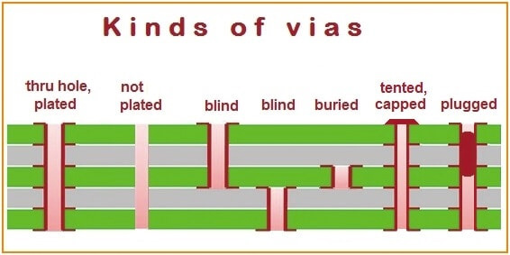
- a through via goes through all the layers. Depending on the cladding in the area where the via is drilled, it may connect to all or just some of the internal layers;
- a blind via goes from the top or bottom layer through one or more layers but is not open at the far end. Plating this via is difficult since a bubble can form at the bottom and prevent proper flow of the solder;
- a buried via connects only internal layers and has no direct access from the top or bottom of the finished board.
Q: What is the diameter of a via?
A: It varies but drilled vias are typically about 0.010 inches (10 mils) in diameter; some boards use laser-drilled vias which are only 3-4 mills. These narrower vias can actually be placed next to the pads of tiny ICs, or under the ICs.
Q: Seems like a big deal about a small hole, am I missing something?
A: Vias are so important that books have been written about their placement, design, and fabrication, as well as their mechanical, thermal, and electrical characteristics. They may look straightforward, but they have many subtleties in all aspects of creation and use.
Q: This sounds complicated…what are the prototype troubleshooting and repair considerations?
A: Multilayer boards and vias are complicated: the tolerances for each layer and of the stack assembly are very tight. But it is being done effectively and consistently due to the automation and robotics associated with every aspect of board fabrication and layer alignment.
Due to the complexity and cost of these boards, it is customary to do 100% bare-board testing before the board is loaded with components. It is difficult if not impossible, to access or repair the inner layers, and the same applies to repair. Once the board is loaded and soldered with its components, issues with internal layers are very difficult to assess, diagnose, or repair (unless special provisions such as access areas are provided in advance). Boards can sometimes be repaired using a laser “knife,” but it is still risky and costly with significant hands-on effort and time required.
Q: How many layers are possible, beyond four layers?
A: The four-layer multilayer board is most common, but some designs use eight or more layers, with 20 layers being the most-common feasible maximum. The high-count multilayer boards are costly to design, difficult to fabricate, and have a scrap rate which can be significant.
Part 4 concludes with some fabrication issues and a look at substrates which have performance capabilities beyond that of FR-4.
References
- Wikipedia, “FR-4”
- PCB trace calculators: MustCalculate, Bittele Electronics Inc. and Trance-Cat
- Wikipedia, “Printed circuit board”
- Wikipedia, “Via (electronics)”
- SEEED Studio, “Printed Circuit Board(PCB) Material Types and Comparison”
- Al Wright, Epec LLC., “PCB Vias – Everything You Need To Know”
- Microwaves101, “FR-4”
- All About Circuits, “Which Via Should I Choose? A Guide to Vias in PCB Design”
- Rogers Corp., “Evaluating PCB Plated Through Holes For 5G Applications”
- John W. Schultz, Compass Technology Group, “A New Dielectric Analyzer for Rapid Measurement of Microwave Substrates up to 6 GHz”
- Rogers Corp., “Characterizing Circuit Materials at mmWave Frequencies”
- Rogers Corp., “Laminate Materials Simultaneously Increase μ and ε, Reducing Antenna Size”
Related EE World Content
- What are RF waveguides? Part 1: context and principles
- What are RF waveguides? Part 2: implementation and components
- Passive microwave components, Part 2: couplers and splitters
- Passive microwave components, Part 1: isolators and circulators
- Next-gen laminates improve insertion loss in automotive radar sensor applications
- High-impedance laminates help reduce antenna size
- Laminates for 5G and other millimeter-wave applications