What is a controlled impedance line? For one thing, the term has to do with Printed Circuit Board (PCB) traces and layouts, which get more complex with higher frequency signals. Generally, you need not worry much about controlling impedance in traces unless you are working with signals at or above 50 MHz. However, most of the interfaces we use today operate at higher than 50 MHz (e.g., USB). When you are designing a PCB, the layout and the length of transmission lines of high speed signals matter.
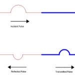
In an ideal world, the signal energy coming out of a pin would travel through PCB traces and be wholly absorbed by the load. However, if energy is not completely soaked up by the load (receiver), residual energy can get reflected back through the PCB trace, reaching the original source of the energy at the output pin (driver). Reflected energy acts like a wave and adds or subtracts to the original signal, causing “ringing.” Resonance can develop at a signal’s characteristic frequency. The result is an unpredictable and confusing signal.
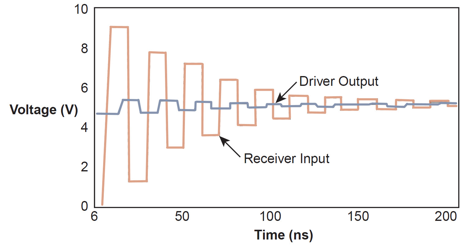
One way to fix this is to have electrically short traces. If the reflected signal is large, it will affect signal integrity with erratic behavior. (Ringing is more prevalent with step signals.) If an output signal is reflected over an electrically short trace, the reflections are likely to be overpowered by the rising or falling edge of the original signal. A rule-of-thumb: an electrically short trace is one that is not longer than one-third the rise time of the signal’s edge. That is, there is vulnerability to ringing if a trace is longer than one-third of the rise time of the step signal. According to Analog Devices’ Dealing with High-speed Logic (PDF), “A more conservative rule is to use a 2-inch (PCB track length)/[per]nanosecond (rise/fall time).” In other words, the signal edge of a high-speed step signal with a rise or fall time of 4 ns will be less prone to problematic ringing if the PCB trace is equal to or less than 8 inches. Others use an even more stringent rule-of-thumb to keep trace length less than one-sixth of the electrical length of the rise time of the signal’s edge.
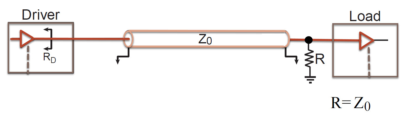
Otherwise, the PCB trace (or track) should be terminated in its characteristic impedance. The unmatched impedance of transmission lines (e.g., PCB traces) can cause reflections as the impedance along the length of the transmission line changes. The source’s impedance needs to match the impedance of the trace and the load. Matching the impedance can be accomplished by tying the trace down with a resistor near the source or the load. Keeping traces short is another way to combat reflections and ringing.
FR4 is a standard material used in PCBs. A signal’s speed in FR-4 travels about six inches per ns (6”/ns). With the most stringent rule to keep trace length less than one-sixth (1/6) of the electrical length of the rise time of the signal’s edge, then signal with a 1 ns rise time would need termination for traces longer than 1 inch.
There are various ways to impedance match. High-speed signals tend to use resistors in series to terminate traces, but high-speed bus lines tend to get terminated with resistance in parallel.
Rough estimating rules can be used in planning stages, but you should do a simulation or the heavy math the old-fashioned way using closed-form transmission line equations. To learn more about reducing ringing and controlled line impedance, consider an application note (AN022) from Pericom (Diodes, Inc.) titled Solutions to High-Speed Board Design (PDF). Other resources include Tektronix’ Fundamentals of Signal Integrity (PDF) and Texas Instruments’ High Speed Layout Guidelines (Rev A) (PDF). PCB layout gets more complicated with higher frequency signals.