By Suresh Patel, Sales Engineer,Mer-Mar Electronics
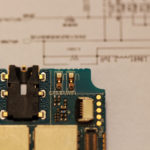
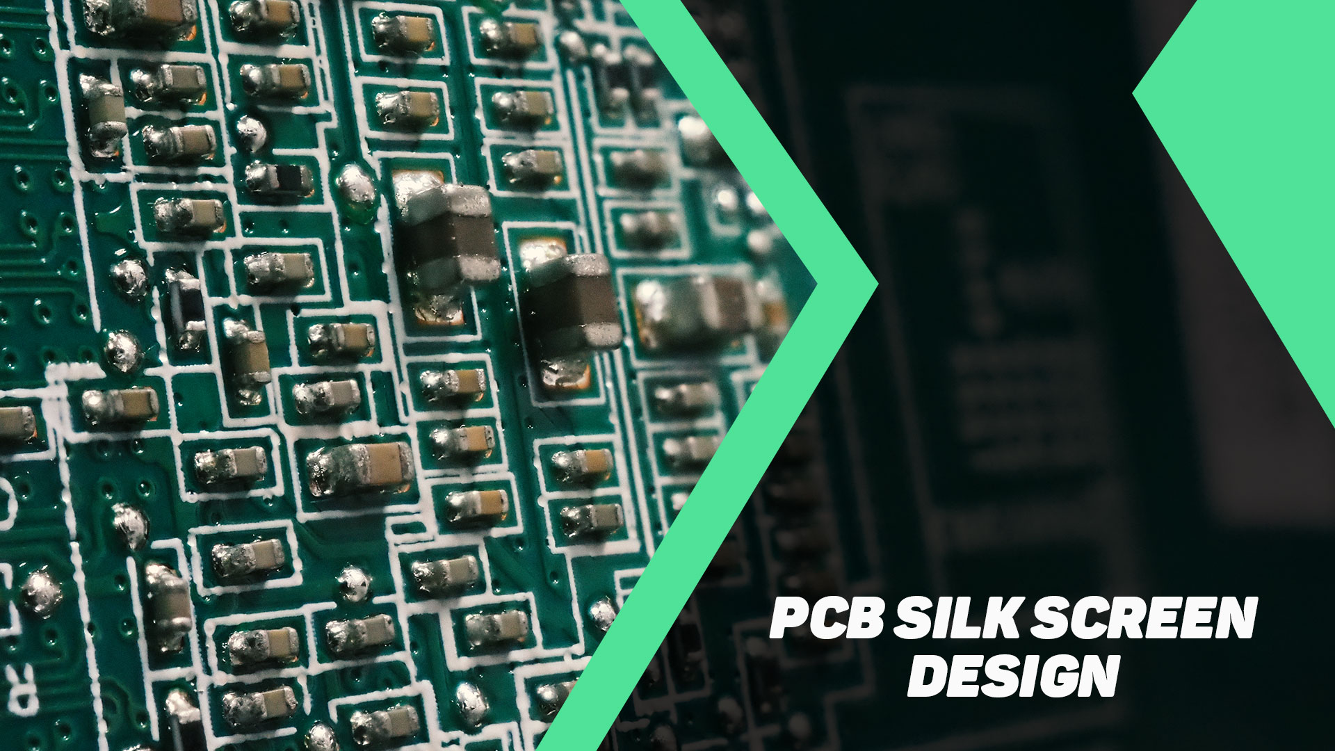
Silkscreen represents the outer layers of a PCB that include text-based readable information such as component reference designator, test points, company logos, PCB part number and version number, etc. This is necessary for circuit board assembly, rework and debug support.
The silkscreen ink is different from the regular printing ink and comes in varied colors like white, black, red, or yellow. Also, the font size depends on the PCB size. The priority should be given to the critical data required to be printed on the silkscreen layer of the PCB.
Earlier, a non-conductive epoxy ink was used in manual screen printing that used a stencil to apply the ink onto the board surface. Recently two techniques are used for printing the PCB silkscreen. They are Liquid Photo Imaging (LPI) and Direct Legend Printing (DLP).
In Liquid Photo Imaging, the PCB laminate is treated with liquid epoxy and dried in Ultra Violet (UV) light. This method is more accurate compared to manual screen-printing. But if the circuit board is complex, it is suggested to use direct legend printing. This method uses acrylic ink and is cured by UV light. Also, this provides the greatest precision and is quite expensive compared to other printing methods.
A PCB silkscreen includes the following vital information required for the assembly and testing of a circuit board.
- Reference Designators indicate the unique location of each component to be assembled on the circuit board.
- Pin marking provides the orientation and polarity details to mount the components on the PCB.
- Certain special components like diodes, optocouplers require component symbols to be printed on silkscreen to ensure proper alignment during component mounting.
- The default switch settings are indicated as instructions on the PCB silkscreen to enhance board usability.
- The pin numbers of dense component packages like a Ball-grid array (BGA) are printed on silkscreen to improve the testing and debug support.
- Test point indicators are marked on the silkscreen to assist the design engineer during PCB testing and debugging.
- The silkscreen also includes caution symbols to highlight high-temperature components that demand user attention.
- Company name, logos, part number, version number, and many such details are also printed on the silkscreen for identification and branding purposes.
Thus, PCB silkscreen is not only used to indicate the component positions but also to provide significant information necessary for successful PCB assembly and efficient testing of a circuit board. PCB designer has to spend enough time to design the correct silkscreen.
Below are the top ten tips to achieve a perfect PCB silkscreen design:
- Font size and line widths: Font size has to be selected based on the PCB dimensions and space availability. It has to suffice the readability requirement in general. Some of the common font sizes used are between 35-50mil. Recommended line width for Reference designators, component pin numbers are not supposed to be less than 6 mils and clearance from PCB pads should be more than 5 mils.
- Silkscreen Reading Orientation: It is suggested to use only two directions in the silkscreen for easy readability. Reference Designators should be oriented such that the layout is readable from left to right and from bottom to top. This makes the silkscreen look uniform and clear.
- Component legend direction: Reference designators should be placed in the same direction as suggested in the silkscreen reading direction. For a horizontally placed component, the reference designator has to be on the left and for a vertically placed component, it has to be on the bottom of the component.
- Component Polarity: Specify the component polarity clearly on the silkscreen for diodes, electrolytic capacitors, and other polarised parts in the same direction within a functional unit to reduce any possible assembly errors. Component failures can be avoided by correct polarity indications on the silkscreen. It is suggested to print the direction and pin numbers of High-speed connectors to assist correct mounting.
- Reference designator positioning: All component reference designators have to be closely placed with the associated components. In case of high component density, it is recommended to place them in groups and label them with pointers.
- Avoid silkscreen markings in critical positions: It is advised not to place any silkscreen markings on top of a component pad which will reduce the solderability of the component. Placing a reference designator or any silkscreen marking under a component symbol will obstruct the readability when the component is mounted.
Also, it is recommended not to place any silkscreen markings on high-speed signal traces to maintain signal integrity.
- PCB mounting hole details: If the PCB is designed to be mounted in a chassis, then the necessary position and dimensional details of the mounting holes have to be provided.
- Avoid silkscreen lines to differentiate solder pads: In the case of two-pin components like resistors, diodes, or capacitors it is seen that a silkscreen line is marked to separate the two pads. This is not recommended as it may cause a solder short on the PCB surface during the soldering process.
- Dense pin-count components: Maintain a minimum of 6 mil clearance between the silkscreen and the pads of dense packaging components like Ball-grid array (BGA) chips.
- Alerts for Quality control: It is necessary to provide caution regarding high-temperature components on the PCB to ensure the overall performance of the circuit.
A good PCB silkscreen adds value to your PCB but comes with an associated cost. Contact your PCB Assembly provider to suggest the right silkscreen printing method for your design.
About the author
Suresh Patel has worked as a Sales Engineer and other management roles at Mer-Mar Electronics. He brings 25 years of experience in printed-circuit-board sales and technical client service and managing business.