We live in a world of solid-state active devices that have made most vacuum tubes obsolete, but a few types remain as they are still indispensable.
Part 1 of this article explained the basics of the photomultiplier tube. This part looks into other PMT characteristics.
Q: Are there solid-state functional equivalents to the PMT?
A: Of course there are, and they work quite well in many applications. These alternatives include the silicon photomultiplier (SiPM), the avalanche photodiode (APD, and the single-photon avalanche photodiode (SPAD). However, each of these has issues, primarily related to internal (intrinsic) noise and sensitivity, that makes each less suitable for some applications. The PMT has the highest internal gain with the lowest internal noise – analogous to SNR – of the available options.
Q: What is the gain of a PMT?
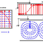
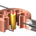
A: It varies, but gain is largely a function of the number of dynodes (Figure 1) and is on the order of 105 to 106 and higher. In contrast, the gain of the basic APD is fairly low, the order of 102. While the apparent gain can be further increased by following it with a conventional low-noise electronic amplifier, the intrinsic noise will be “gained up “as well, and so SNR will not improve. It will actually degrade due to the amplifier’s own added noise.

Q: Is noise the figure of merit for a PMT (or other photodetector)?
A: Noise is one, of course, as is gain, But the other figure of merit is “dark current,” which is the amount of current produced when there are no incident photons. Dark current establishes a noise floor for the device, and the lower the dark current is, the better. A high-end PMT has the lowest dark current of any photodetectors, with its dark current is due to thermal emissions of electrons from the photocathode, leakage current between dynodes, and even stray high-energy radiation
Always keep in many that in many high-end designs from DC to RF (GHz and higher), internal noise is one of the limiting factors in the achievable performance. As in most applications with low signal levels, the SNR of the first stage limits performance, and it’s critical to have a high-gain, low-noise first stage.
Q: Why not just take the small current developed at the cathode, and amplify it using an electronic amplifier?
A: Again, it’s a matter of noise; the photon-derived current is so small that it would be “swamped” by the noise of any electronic amplifier and thus be lost. In contrast, the PMT is a relatively low-noise, low-dark current device.
Q: What is the efficiency of the PMT?
A: Quantum efficiency is the percentage of impinging photons that are converted to electrons at the cathode; a typical value is about 30%. The cathode is key, of course, and its design and thickness involve tradeoffs. If it is too thick, more photons will be absorbed, but fewer electrons will be emitted from the back surface; however, if it is too thin, too many photons will pass through without being absorbed.
Q: Does the PMT require more circuitry than the solid-state alternatives?
A: The difference is modest, but you do need a higher-voltage supply for the dynodes and anode (about 1000 V).
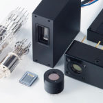
Q: Who are the vendors of PMTs? What are the attributes of a representative PMT?
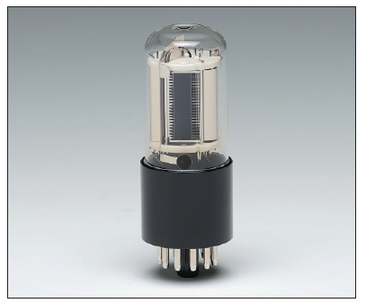
A: There are many vendors of PMTs, among them Hamamatsu Photonics, Photek (UK), Thorlabs, and Newport Corp. The Hamamatsu R3896 is a typical device (Figure 2): it responds to photons in the 180 nm to 900 nm wavelength range using a multi alkali photocathode, has nine dynodes arranged in a circle within an 8 × 24 mm rectangle, and requires an anode bias of 1250 V.
The next part of this article looks at a very different vacuum tube: the traveling wave tube, used as the core element of a high power, mm-wave power amplifier.
References
- EE World, “Magnetron, Part 1: Application and operating principles”
- EE World, “Magnetron, Part 2: History and future”
- Wikipedia, “Photoelectric effect”
- Khan Academy, “Photoelectric effect”
- Encyclopaedia Britannica, “Photoelectric effect”
- Scientific American, “Einstein’s Legacy: The Photoelectric Effect”
- Florida State University, “Concepts in Digital Imaging Technology: Photomultiplier Tubes”
- Hamamatsu Photonics, Photomultiplier Tubes: Basics and Applications,
- Hamamatsu Photonics, Data sheet Hamamatsu R3896
- EE World, “What are RF waveguides? Part 1: context and principles”
- EE World, “What are RF waveguides? Part 2: implementation and components”
- Radar Tutorial/EU. “Traveling Wave Tube” (very good description and images)
- Elsevier Science Direct, “Traveling Wave Tube”
- Tutorials Point, “Travelling Wave Tube” (readable, somewhat simplified)
- Microwaves 101, “Traveling Wave Tubes” (has close-in photos of custom made, non-commercial TWTs)
- Engineering and Technology History Wiki, Rudolf Kompfner
- Microwave Journal, Military Microwaves Supplement, “TWTAs Still Dominate High-Power and mmWave Applications”
- dB control/Heico, “What’s Better – TWTAs or SSPAs?
- Greek Microwave Group, “TWTs vs SSPAs”
- Microwave Journal, “ABI Research Finds Microwave Tube Market Still Strong at Over $1B for 2018”
- Semantic Scholar, “Communication satellite power amplifiers: current and future SSPA and TWTA technologies”