Microelectromechanical systems (MEMS) has several names, including micro-electro-mechanical systems, and micromechatronic systems. In Japan, MEMS is called micromachines, while in Europe, it’s referred to as microsystem technology (MST). Whatever name that’s used, MEMS devices are made using components measuring from 1 to 100 μm (0.001 to 0.1 mm), with MEMS devices ranging from 20 μm to 1 mm. There are exceptions, such as large digital mirror arrays that are much larger.
This FAQ briefly compares MEMS with conventional mechanical structures and molecular nanotechnologies, looks at MEMS technology categories and common applications, and closes by considering a range of emerging applications, including power electronics, 5G and 6G communications, the metaverse, and new uses for medical MEMS.
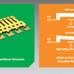
MEMS are different, and those differences are important in determining where and when MEMS is appropriate to use. Compared with conventional mechanical devices, MEMS have a large surface area to volume ratio, and the forces produced by electrostatic charges and magnetic moments are more important. And at the MEMS scale, fluid dynamics such as surface tension and viscosity are important design considerations in many systems. Compared with molecular electronics or nanotechnology, MEMS does not generally need to take surface chemistry into consideration. MEMS technology can be used for a range of devices, from pumps to inductors. Switch technology presents a good example of basic MEMS implementation and can use ohmic or capacitive designs.
Ohmic MEMS switches employ electrostatically controlled cantilevers. Their lifetimes are determined by the occurrence of metal fatigue of the cantilever, contact wear, and cantilever deformation. Capacitive MEMS switches use a sensing element such as a moving plate that changes capacitance and activates the switch.
MEMS is a well-established, but still advancing, commercial technology. Various sensors to monitor vibration, temperature, light, and linear and rotational movement and acceleration are some common MEMS applications. They can be found in military equipment, mobile phones, vehicles, and industrial and communications systems. In the medical field, so-called bioMEMS are used to sense biological functions, and to deliver drugs and other therapies. In industrial and automotive settings, they are used to monitor vibration and help prevent failures by providing early warning of potential malfunctions and breakdowns. In telecommunications, MEMS are used as switches, and in tunable lasers, tunable filters, optical switches, dynamic gain equalizers, attenuators, and other applications (Figure 1).

MEMS for power electronics
Miniaturization of power converters for wearables, implantable electronics, and IoT devices is one of the drivers for the development of MEMS inductors. The goal is increased integration using power supply in package (PwrSiP) and power supply on chip (PwrSoC) technologies to design tiny power supplies that deliver high efficiencies, resulting in high power densities.
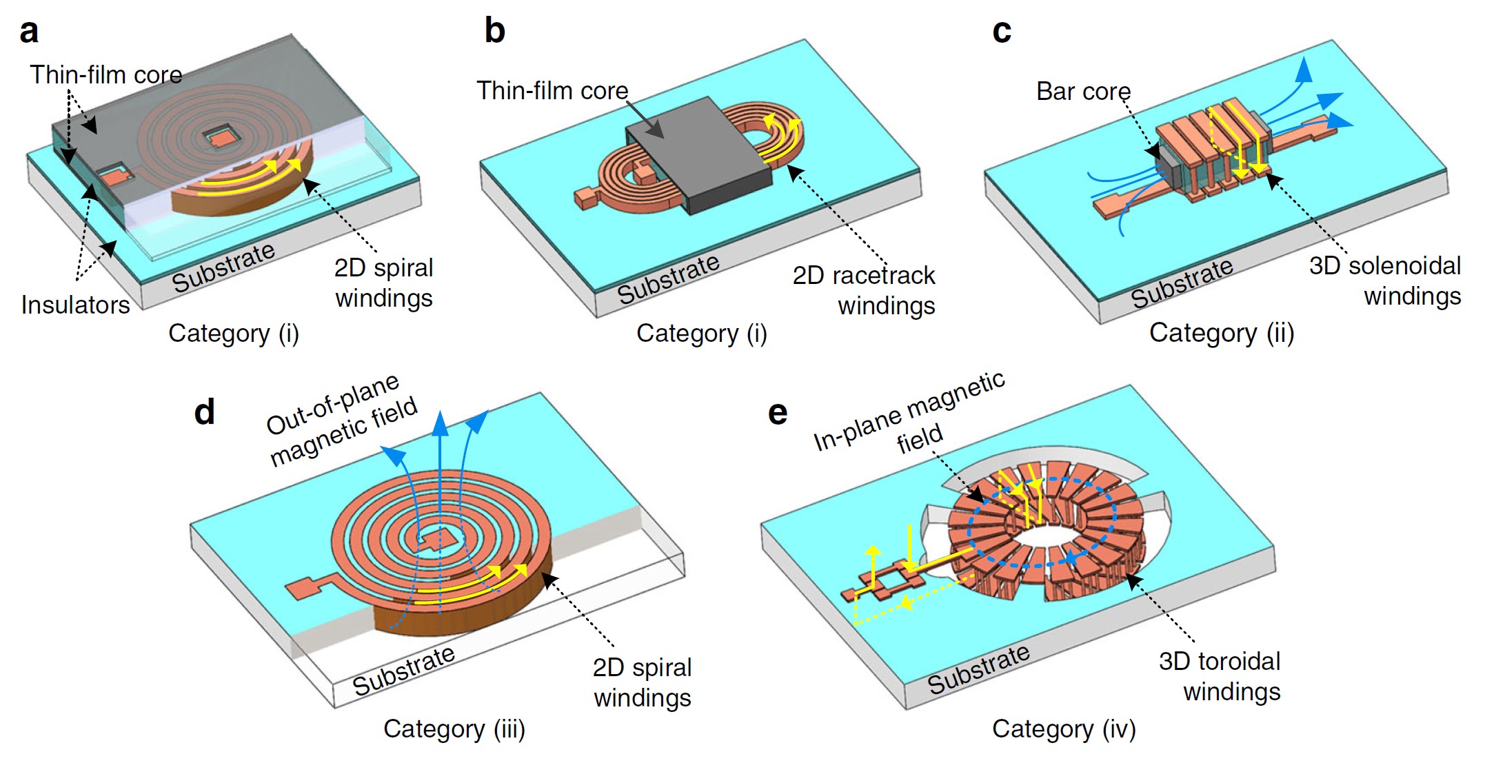
MEMS inductors can be classified in several ways, such as operating frequency, power handling, and geometry. One common classification is based on the position of the windings relative to the substrate and their shape, including (Figure 2): (i) 2D inductors on-substrate, further subdivided into spiral inductors (a) and racetrack inductors (b); (ii) 3D on-substrate solenoidal inductors with a magnetic bar core (c); (iii) 2D in-substrate spiral inductor (d), and; (iv) 3D in-substrate toroidal inductor (e).
Challenges remain for fabrication of MEMS inductors. Air-core MEMS inductors can be used at frequencies above 22 MHz (the VHF range) but magnetic cores are needed for lower frequencies. Unfortunately, while it’s possible to use gallium-nitride (GaN) power semiconductor devices to design VHF power electronics, magnetics materials have not kept up and their large core losses are a constraining factor in the development of VHF power converters.
PwrSoC integration efforts are turning to MEMS packaging technologies to enable the fabrication of miniature power converters. Approaches being explored include 2D/2.5D packaging that uses wire bonding or flip-chip techniques and 3D packaging using vertical stacking of ICs and through-silicon-via-based Si interposers. As in the case of magnetic materials, these MEMS-based packaging technologies are not ready for commercial exploitation.
MEMS for beyond 5G RF
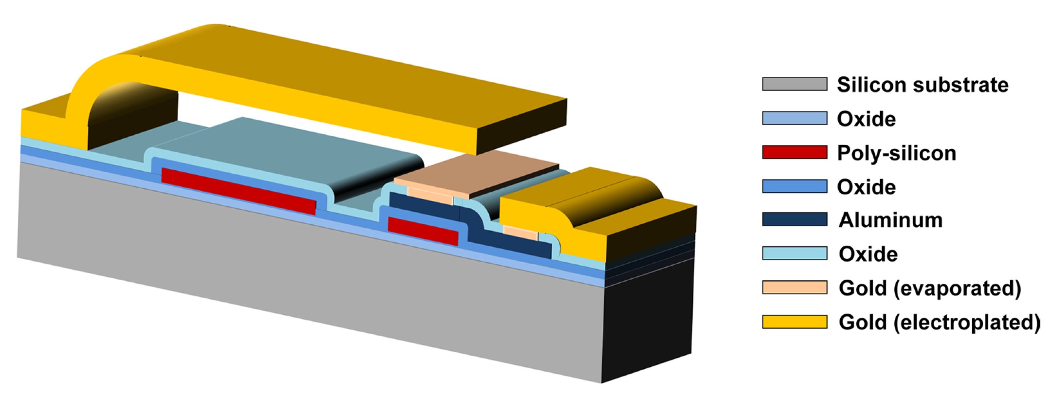
Radio frequency MEMS (RF-MEMS) are passive components such as attenuators that provide improved performance, including better isolation, lower power dissipation, smaller and lighter weight, and lower cost for use in multi-GHz applications. Recently, RF-MEMS have been fabricated using a surface micromachining process that uses two conductive thin-film layers protected by polycrystalline silicon (poly-silicon) and aluminum, above which the actual MEMS suspended electrostatically-driven membranes are built using electroplated gold (Figure 3). In addition, the metal-to-metal contact resistance is minimized using a thin film of evaporated gold.
The demand for ever-smaller and higher-performance multi-GHz components is driving the development of RF-MEMS technology. RF-MEMS devices are being developed to help address challenges such as very low end-to-end latency, expected to drop from 5 ms in 5G to 1 ms in 6G, plus the demand for shrinking massive MIMO (mMIMO) technology into large intelligent surface antenna (LISA) technology. LISA will use RF-MEMS technology in a two-dimensional artificial structure with a large number of individually-controlled reflective-surface/antenna elements to enable mMIMO capability to fit into smaller systems operating in the 30 to 300 GHz range for critical applications such as vehicle-to-vehicle communications, remote surgery, and massive machine-to-machine communications in Industry 4.0.
pMUTs and the metaverse
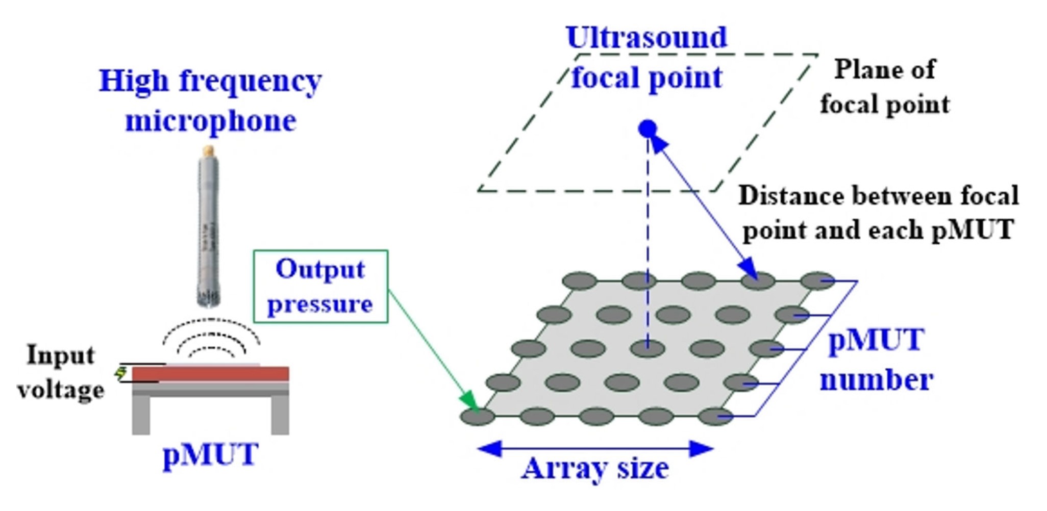
Haptic feedback uses force, an electric signal, or acoustic pressure to create a tactile sensation. Air-coupled ultrasonic transducers are used in current designs, but they are too bulky for widespread adoption. Instead, piezoelectric micromachined ultrasonic transducers (pMUTs) are being developed. pMUTs will have the same 40 kHz resonant frequency as today’s air-coupled ultrasonic transducers, but are much smaller, with low power consumption. Lead zirconate titanate (PZT) is used as the piezoelectric layer and is deposited using RF sputtering. The resonant cavity is formed by using deep reactive ion etching to release a circular membrane. These pMUTs are intended to be used in large arrays (Figure 4). A single pMUT can produce an acoustic pressure of 0.227 Pa when driven with 70 V peak-to-peak.
Haptic feedback is not the only potential application for pMUTs in the Metaverse. With appropriate modifications to the design, pMUTs are expected to be used for levitation, particle manipulation, and photoacoustic imaging. Earlier efforts to develop pMUTs used polyvinylidene fluoride (PVDF) as the piezoelectric layer. The piezoelectric coefficient of PVDF proved to be too low to generate the needed acoustic pressure to create an ultrasound-based tactile effect. PZT has the required piezoelectric coefficient and can be fabricated into pMUTs suitable for integration into portable devices using existing production equipment.
bioMEMS, μMS, and CMUTs
Microfluidics and bioMEMS devices are being used for a range of medical applications, including sample preparation, DNA extraction, amplification, and identification, plus implanted and transdermal bioMEMS devices that can be remotely configured to automate and control drug delivery using micro-needles, MEMS reservoirs, micro-pumps, and actuators.
Micromagnetic stimulation (μMS) uses implanted MEMS microcoils to produce a magnetic field for localized transcranial magnetic stimulation (TMS). MEMS coils are small enough to be directly implanted into the brain. They are expected to facilitate confined activation of narrow regions of the brain and enable a micromagnetic stimulation inductor for neural prosthetics.
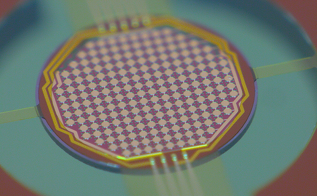
Capacitive micromachined ultrasonic transducers (CMUTs) have been developed to augment and replace today’s PZT-based transducers. CMUTs fabricated on CMOS wafers (CMUT-on-CMOS) enable larger bandwidths, fabrication of large arrays with integrated drivers, and enable high volume ultrasound transducer production with lower costs (Figure 5). CMUT-on-CMOS is a high frequency (1 to 50 MHz) ultrasonic technology and is enabling high-resolution 3D medical imaging and the development of ultra-small imagers that can fit inside a catheter.
Summary
MEMS is an established technology that operates using fundamentally different mechanisms compared with conventional mechanical devices and molecular-sized devices. MEMS devices are already widely dispersed in communications, transportation, military, industrial, and consumer applications. The technology is continuing to advance for emerging applications in power conversion, the metaverse, 6G telephony, and advanced medical diagnostics and therapeutics.
References
Biochips, Atomica
Capacitive micromachined ultrasonic transducers, Philips Engineering Solutions
Exploitation of response surface method for the optimization of RF‑MEMS reconfgurable devices in view of future beyond‑5G, 6G and super‑IoT applications, Nature Scientific Reports
Investigation of Achieving Ultrasonic Haptic Feedback Using Piezoelectric Micromachined Ultrasonic Transducer, MDPI electronics
Microelectromechanical systems, Wikipedia
MEMS inductor fabrication and emerging applications in power electronics and neurotechnologies, Microsystems and Nanoengineering