By Suresh Patel, Sales Engineer, Mer-Mar Electronics
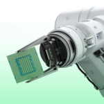
 The Boundary-scan, aka JTAG (Joint Test Action Group), is the IEEE 1149.1 standard used to verify and test Integrated Circuits (IC) interconnections on the PCBs. Using the boundary scan in PCB production will effectively reduce manufacturing costs, accelerate test automation, and improve PCB quality with better fault coverage. The growing circuit complexity has increased the board space constraints and accessibility issues in fine-pitch and BGA components. The cost of using In-circuit test (ICT) fixtures will be expensive in such dense PCB assemblies.
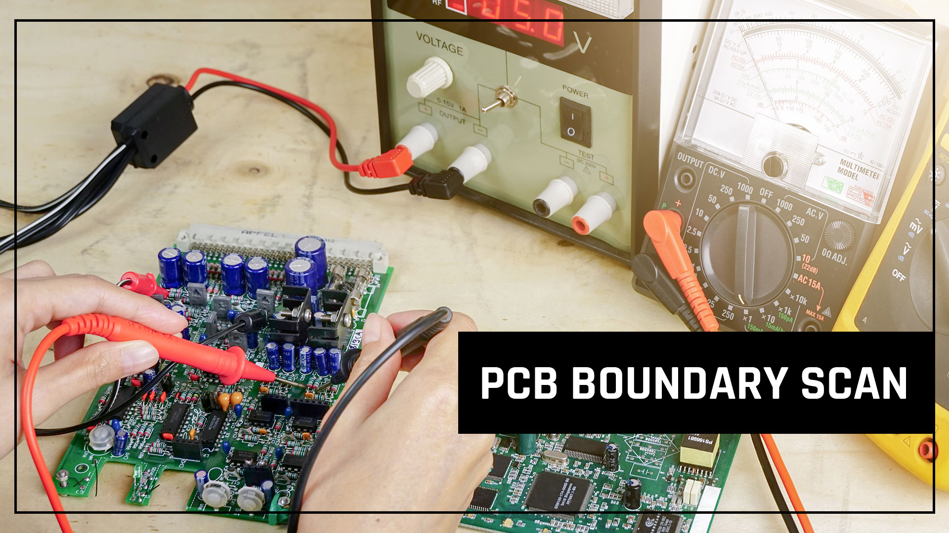
To ensure the product quality, it is important to test assembled PCBs for several factors like component mounting, soldering connections, functional accuracy, etc. Generally, a combination of visual inspection and functional tests is conducted to obtain maximum fault coverage. The PCB defect range is categorized using a popular method known as PCOLA/SOQ/FAM, which evaluates structural and functional parameters. If you are wondering what PCOLA/SOQ/FAM is, here’s the explanation.
PCOLA:
- Presence: Inspect if the component is mounted.
- Correctness: Inspect if the right component is mounted.
- Orientation: Inspect if the component polarity and direction are correct.
- Live: Inspect if the component is active and responds to a stimulus.
- Alignment: Inspect if the component is mounted within footprint margins.
SOQ:
- Shorts: Check if there is a wrong connection from one IC pin to another pin.
- Opens: Check if there is a missing connection from one IC pin to another pin.
- Quality: Check if the IC connection is as per set quality standards.
FAM:
- Features: Verify if the IC feature is working.
- At speed: Verify if the IC connection operates in the expected speed range.
- Measurement: Verify if the connection attributes are measurable.
Boundary-scan testing can detect most PCB defects in the above categories and provides optimum coverage. It’s essential to test after PCB Assembly is done. Though there is some infrastructure cost involved in this method, there are multiple benefits like increased product yield, reduced test time, reusable test patterns, etc.
What is a boundary scan, and how does it work?
The boundary scan or JTAG (Joint Test Action Group) is used to verify the designs and test PCBs for any defects. A JTAG-compatible IC includes boundary-scan cells between a core logic and the signal Input/Output (IO). These boundary scan cells can be either input only, output only, or bidirectional cells. They are placed at the boundaries of an IC and hence are known as boundary-scan cells. They are transparent cells during the normal operation of the chip. But, in the test mode, the input pin’s status is read, and the output pin status is controlled by the boundary scan cells. The boundary scan cells are connected serially, and test vectors are used to check the board interconnections.
An IC that conforms with the JTAG standard should include the following:
- A boundary-scan cell at every Input and Output pin.
- Serial boundary scan cells to define a scan path.
- A Test Access Port (TAP) controller with JTAG signals- Test Clock (TCK), Test Mode State (TMS), Test Data Input (TDI), Test Data Output (TDO), and Test Reset (TRST). The first four JTAG signals are mandatory, and TRST is an optional signal which can be used to reset the TAP controller.
- Five Additional pins on the IC to connect the JTAG signals to the scan chain.
- The vendor provided Boundary Scan Description Language (BSDL) file describing the component’s behavior, package details, instructions, and other necessary information to build the test program.
Using the boundary-scan test vectors, we can verify the connections between ICs on a circuit board without needing to probe the pins physically. A boundary-scan cell at each pin of the IC includes a latch and multiplexer circuit that either captures data from an input pin or feeds data to an output pin. The scan chain controls the transfer of test vectors based on the instructions provided by the TAP controller. The test vectors can be reprogrammed with multiple test instructions to increase the fault coverage. The boundary-scan method can decrease the test time significantly with improved diagnostic capabilities and reduced infrastructure costs.
Why manufactured PCBs should be boundary scanned?
The manufactured PCBs should be tested for their functionality before shipping to the customers. The performance quality of the PCB drives the overall product sales. Boundary-scan testing offers several advantages, which makes it one of the best methods for testing PCB assemblies.
- Decreases the design iterations
In the PCB prototyping stage, testing the circuit functionality is essential, but using ICT fixtures may not be viable as the design is not yet stabilized. Instead, boundary scan testing can help manufacturers to verify the design performance faster and increase the output. This will further reduce the iterations in the design cycle and enable the product to be mass produced.
- Test vectors can be re-utilized.
In the Boundary-scan method, the same test vectors can be reused in different scenarios, like the vectors applied at the chip level can be re-applied at the board level or even system-level testing. This will save the cost compared to the ICT method, where a different set of test fixtures may be required.
- ROI is quicker compared to ICT
Though boundary scan testing requires an investment in the test setup infrastructure, the return on investment will be faster with the addition of new test projects. It is possible to program and debug ICs like CPLD, FPGA, EEPROM with memory, Flash devices, etc., using the JTAG setup.
- Reduced test time with efficient debug capabilities.
Automated debugging and testing can reduce the possibility of fault introduction due to manual handling. JTAG method can track any PCB fault up to the IC pin level and hence speeds up the debug process. Also, the boundary scanning of vital components like onboard processors and memory devices can reduce the functional test time. This improves product quality and output.
- Faster product-to-market timelines
Since the boundary scan method can drastically reduce the PCB test time, the quick time to market will greatly benefit a highly competitive electronics market. The product manufacturers can generate a high business value using the JTAG test method.
- Cost-effective production
The reduced count of test pins in the JTAG testing method provides a great advantage compared to the ICT Bed-of-nails technique. The common test interface across all board types will reduce the cost of adapters, fixtures, etc.
Conclusion
There are several merits in using boundary-scan testing for manufactured PCBs. It provides an economic test process with higher production yields. It can scale up to functional testing and debug support also. The overhead of extra design efforts has to be considered from the early PCB development stages. The increasing demand for PCB miniaturization and associated structural testing can be accomplished using the boundary scan test technique.