Modern zero-drift amplifiers provide the extremely low drift and noise performance needed for processing many optical biological, and physical-world signals near 0 Hz.
In our world of ever-faster, wider-bandwidth signals and systems operating at higher and higher frequencies, it may seem that signals in the very-low-frequency range — down towards zero hertz (0 Hz) — are either trivial to deal with or an anachronism.
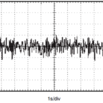
However, that’s just not the case at all. There are many real-world phenomena that exist and provide critical information in that span of the spectrum. For example, consider something as commonplace and ubiquitous as monitoring outside temperature over the course of a day. While the temperature may swing over ten or twenty degrees over a 24-hour period, the rate at which it changes is very slow (Figure 1).

Similarly, observing light intensity from a glowing candle flame as it flickers, burns higher, and then eventually burns out is a slow-moving situation. There are many other examples of such slow-moving signals: patient monitoring of various body parameters, bridge movements, thermal expansion, and contraction are just a few.
Amplifying these signals to their sensor should be easy; after all, we have amplifiers and analog front ends that can go to the hundreds of megahertz and multi-gigahertz range, so what’s the problem?
Amplifying these ultra-slow signals is challenged by two factors: amplifier/analog front end (AFE) drift and noise. Drift is a shift in baseline created due to various thermal effects, while noise has many sources.
All amplifiers have some drift in their low-frequency performance, largely but not entirely due to thermal effects as well as shifts in operating points as current and voltages change. Signal-chain performance is degraded by any initial DC offset in the amplifier’s parameters, such as bias current or voltage offset, and inherent 1/f (pink) noise, as well as subsequent unavoidable performance shifts due to temperature-induced drift, power-rail variations or component.
Devising an amplifier that can amplify ultralow-frequency signals with zero or near-zero drift and offset other errors, as well as low passband noise, is a unique challenge. Low-frequency drift and noise can be filtered out from high-frequency signals, but when the noise and drift are in the same band as the signal, filtering obscures the changes of interest.
The alternative to filtering is an amplifier topology which is specifically designed for ultralow frequencies from DC to several hundred hertz or even a few kilohertz. Note that these amplifiers are sometimes called “DC amplifiers” since their bandwidth extends down to DC, but it’s not really DC that they need to amplify. After all, a true DC signal is constant and thus conveys no information, so there is no need to amplify it. Still, the term “DC amplifier” is often used for these devices.
Low-drift amplifiers fill the void
The problem of capturing and amplifying signals at these extremely low frequencies is not new; in fact, it has been around since the pre-electronic and pre-electricity days when researchers needed to somehow capture changes in parameters such as light. They devised schemes to mechanically “chop” the desired signal at a much higher rate, thus modulating it up to part of the spectrum where it could be passed along, then demodulated by a synchronized chopper at the other end recording and observing. The low-frequency drift was effectively filtered out and irrelevant (there’s more of this mechanical chopping later).
This chopping concept was soon extended when vacuum tubes came along and electronics as we know them began. These vacuum-tube-based chopper amplifiers worked well but had all the limitations of tube technology of the time: size, weight, and power requirements were high. As transistors and analog ICs became standard components, they were soon used in chopper-topology amplifiers to capture and amplify these signals.
One consequence of this evolution of the chopping technique for low-frequency signals was that the term “chopper amplifier” became synonymous with the somewhat-more correct term “DC amplifier,” the more-accurate term “low-frequency amplifier” or, best of all, “zero-drift amplifier” (recognizing that no amplifier has truly zero drift, but the right design can come very close to zero). Keep in mind that chopping is a technique and topology, not the objective of zero-drift — so using the term indicating what it is to also mean what it accomplishes can be confusing.
Two topologies are used to achieve “zero-drift” performance:
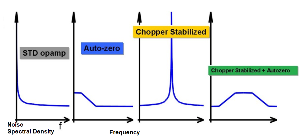
- Chopping, as previously noted, uses signal modulation and demodulation and has lower baseband noise, but also produces noise artifacts at the chopping frequency and its harmonics.
- Alternatively, auto-zeroing uses a sample-and-hold circuit and is suitable for wider-band applications but has more in-band voltage noise due to noise “foldback” to the baseband part of the spectrum.
Advanced zero-drift amplifier ICs combine both techniques to offer the “best of both worlds.” They manage the noise spectral density (NSD) to offer lower baseband noise while minimizing high-frequency errors such as ripple, glitches, and intermodulation distortion (IMD) (Figure 2).
Chopping has its attributes
This amplifier, more formally known as a chopper-stabilized amplifier (but usually called a chopping amplifier or just a “chopper”) uses a chopping circuit to break up (chop) the input signal so that it can be processed as if it was a modulated AC signal. It then demodulates the signal back to a DC signal at the output to extract the original signal.
In this way, extremely small DC signals can be amplified while the effects of unwanted drifts are greatly minimized to near zero. The chopping modulation separates offset and low-frequency noise from the signal content by modulating the errors to higher frequencies, where they are much more easily minimized or removed via filtering.
Chopping operation details are easily understood in the time domain (Figure 3). The input signal (blue waveform — a) is modulated by chopping (b) to a square wave. That signal is demodulated (c) at the output (d) back to DC. The inherent low-frequency errors (red waveform) in the amplifier are (c) modulated at the output to a square wave, which is then (d) filtered by a low-pass filter (LPF).
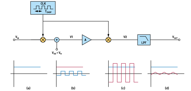
Of course, no technique is perfect, and that applies to chopping as well. There are artifacts due to the chopping (switching) action, as well as noise induced by the edges of the chopping clock. Even though the chopper design adds internal filtering to reduce the artifacts and noise, some of these remain. Nonetheless, a high-performance chopper will have drift and noise which is an order of magnitude or better (less) than a high-end bipolar amplifier which typically offers offset voltages of about 25 μV and drift of 0.1 μV/°C.
The next part explores the auto-zeroing approach to implementing a zero-drift amplifier.
EE World-related content
Understanding the lock-in amplifier, Part 1: The sensing challenge
Understanding the lock-in amplifier, Part 2: The homodyne solution
Lock-in amps get AM/FM modulation option
Teaching instrumentation gets new filter options, lock-in amp
Squash 1/f noise with zero-drift amplifiers
New 45-V, zero-drift op amp features ultra-high precision and EMI filtering
Zero-drift, nanopower op amp works from 650 nA supply current
Zero-drift Amplifier Achieves Industry’s Lowest Voltage Noise
Tiny 3-MHz chopper op amps feature rail-to-rail input and output
Additional references
Analog Devices, “How to Use Zero-Drift Amplifiers in Wider Bandwidth Applications”
Analog Devices, Tutorial MT-055, “Chopper Stabilized (Auto-Zero) Precision Op Amps”
AZO Optics, “What is an Optical Chopper?”
Perkin Elmer, AN-1003, “Low Level Optical Detection using Lock-in Amplifier Techniques”
Ophir Optronics Solutions Ltd, “Working in the Basement: Measuring Signals Below the Noise Floor with a Lock-in Amplifier”
Stanford Research Systems, “SR542 — Low jitter optical chopper”