Modern zero-drift amplifiers provide the extremely low drift and noise performance needed for processing many optical biological, and physical-world signals near 0 Hz.
The ultimate limitations of chopping led designers to investigate another approach called auto-zeroing, which is especially feasible with integrated circuits. This is a dynamic correction technique that works by sampling and subtracting low-frequency error sources in an amplifier.
A basic auto-zero amplifier consists of an amplifier with its unavoidable offset and noise, electronic switches to reconfigure the input and output, and an auto-zero sampling capacitor (Figure 1).
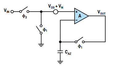
During the auto-zero phase (ϕ1) the circuit’s input is shorted to a common voltage, and the auto-zero capacitor samples the input offset voltage and noise. The amplifier is “unavailable” for signal amplification during this phase, as it is occupied with another task. To overcome this and allow an auto-zeroed amplifier to operate in a continuous manner, two identical channels must be interleaved in what is called “ping-pong” auto-zeroing, which is invisible to the user.
During the amplification phase (ϕ2) the input is connected back to the signal path and the amplifier is again available for amplifying the signal. The low-frequency noise, offset, and drift are canceled by auto-zeroing, and the remaining error is the difference between the current value and the previous sample of the errors.
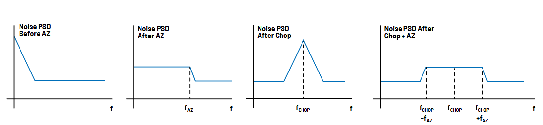
Since low-frequency error sources do not change much from ϕ1 to ϕ2, this subtraction works well. The high-frequency noise, however, is aliased down to the baseband and results in an increased white-noise floor (Figure 2).
How good is auto-zeroing compared to a very good precision op amp? The performance of advanced auto-zeroing IC amplifiers is impressive, they are typically better than even a “very good” precision op amp by two orders of magnitude in critical offset, drift, and noise specifications. Thus, while their numbers are obviously not zero, they are very close to it.
For example, the Analog Devices ADA4528 is a single-channel, rail-to-rail (RTR) zero-drift amplifier that features an offset voltage of 2.5 microvolts (μV) (maximum), offset voltage drift of just 0.015 μV/°C (again, maximum), and voltage noise density of 5.6 nanovolts (nV)/√Hz (at f = 1 kHz, gain of +100) and 97 nVpeak-peak (for f = 0.1 Hz to 10 Hz, gain of +100). Another Analogs Devices zero-drift amplifier, The ADA4522, offers an offset voltage of 5 μV (maximum), offset voltage drift of 22 nV/°C (maximum), voltage noise density of 5.8 nV/√Hz (typical) and 117 nV (peak-to-peak) from 0.1 Hz to 10 Hz (typical), along with input bias current of 50 picoamps (pA) (typical).
Getting even better
By careful examination and investigation of the root cause of each of the subtle sources of errors, designers of zero-drift ICs have been able to devise advanced or sophisticated topologies and process approaches to overcome them. Not only do these reduce the magnitude of these artifacts but they also place them at higher frequencies where they are easier to filter out at the system level. Among the second-order sources of imperfection are these two:
Ripple — a basic consequence of the chopping modulation technique that moves these low-frequency errors to odd harmonics of the chopping frequency.
Glitch Artifact — transient spikes that are caused by charge injection mismatch from the chopping switches. The magnitude of these glitches depends on many factors including source impedance and the amount of charge mismatch.
There’s good news and bad news as these impressive zero-drift amplifiers have been developed. The good news is that drift and offset errors have been reduced by orders of magnitude compared to a high-precision conventional amplifier. The bad news is that just as when a river dries up in a drought, and new riverbed features are revealed for the first time, the near-total elimination of first- and second-order errors allows the tiny, residual third-order error sources of all types and sources now become visible.
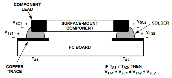
For example, for zero-drift amplifiers and their analog-signal channels, one potential source of offset error is the Seebeck (thermocouple) voltage on the circuit board which occurs at the junction of two dissimilar metals and is a function of the temperature of the junction. The most common metallic junctions on a circuit board are solder-to-board trace and solder-to-component lead.
Consider the cross-section of a surface-mount component soldered to a printed circuit board (Figure 3). A variation in temperature across the board, such as with TA1 different than TA2, causes a mismatch in the Seebeck voltages at the solder joints, thereby resulting in thermal voltage errors that degrade the ultralow offset voltage performance of the zero-drift amplifiers.
Minimizing these thermocouple effects requires extraordinary attention to seemingly insignificant details. For example, resistors should be oriented so that the various heat sources warm both ends equally. Where possible, the input signal paths must contain matching numbers and types of components to match the number and type of thermocouple junctions. Placing matching components in close proximity and orienting them, in the same manner, will ensure equal Seebeck voltages, thus canceling thermal errors.
Heat sources on the board should be kept as far away from the amplifier input circuitry as practical. Further, a ground plane can be used to help distribute heat throughout the board to maintain a constant temperature across the board and so reduce EMI noise pickup.
The next part visits the mechanical chopper — the forerunner of electronic zero-drift amplifiers — which is still in widespread use.
EE World Related Content
Lock-in amps get AM/FM modulation option
Teaching instrumentation gets new filter options, lock-in amp
New 45-V, zero-drift op amp features ultra-high precision and EMI filtering
Zero-drift, nanopower op amp works from 650 nA supply current
Zero-drift Amplifier Achieves Industry’s Lowest Voltage Noise
Tiny 3-MHz chopper op amps feature rail-to-rail input and output
Additional References
Analog Devices, “How to Use Zero-Drift Amplifiers in Wider Bandwidth Applications”
Analog Devices, Tutorial MT-055, “Chopper Stabilized (Auto-Zero) Precision Op Amps”
AZO Optics, “What is an Optical Chopper?”
Perkin Elmer, AN-1003, “Low Level Optical Detection using Lock-in Amplifier Techniques”
Ophir Optronics Solutions Ltd, “Working in the Basement: Measuring Signals Below the Noise Floor with a Lock-in Amplifier”
Stanford Research Systems, “SR542 — Low jitter optical chopper”