
This article introduces the VCM vs. VOUT plot for an instrumentation amplifier with two operational amplifiers (op amps) and delivers a thorough treatment of this amplifier topology. Additionally, the internal node equations are derived and used to plot each internal amplifier’s input common-mode and output-swing limits as a function of the instrumentation amplifier’s common-mode voltage. Finally, a software tool that simulates the VCM vs. VOUT plot is introduced.
Peter Semig, Analog Applications Engineer, Texas Instruments, Inc.
The most common issue found in the TI E2E™ Community (online support community for Texas Instruments) for instrumentation amplifiers involves interpreting the datasheet plot for common-mode voltage versus output voltage (VCM vs. VOUT). Misinterpretation or misunderstanding this plot results in forum posts that describe distorted output waveforms, incorrect device gain, or ‘stuck’ outputs. Verifying that the device is operating within the limits of the VCM vs. VOUT plot is always the first thing I check when responding to an application issue.
The VCM vs. VOUT plot
The input common-mode and output-swing limitations of all internal amplifiers of an instrumentation amplifier are represented in the VCM vs. VOUT plot.
A typical VCM vs. VOUT plot for a two-op-amp instrumentation amplifier is shown in Figure 1. The interior of the plot defines the linear operating region of the instrumentation amplifier because each line in the plot corresponds to either an input or output limitation of one of the two internal amplifiers. The VCM vs. VOUT plot is specified for a particular supply voltage, reference voltage, and gain as shown in Figure 1.
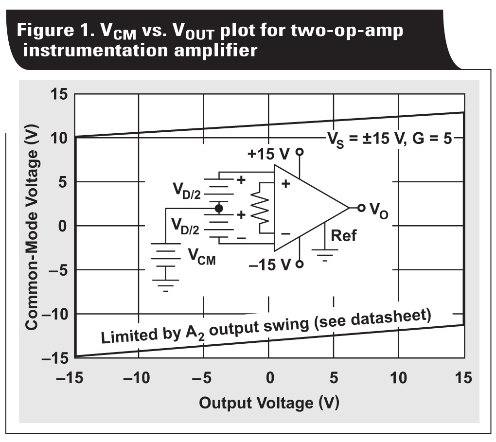
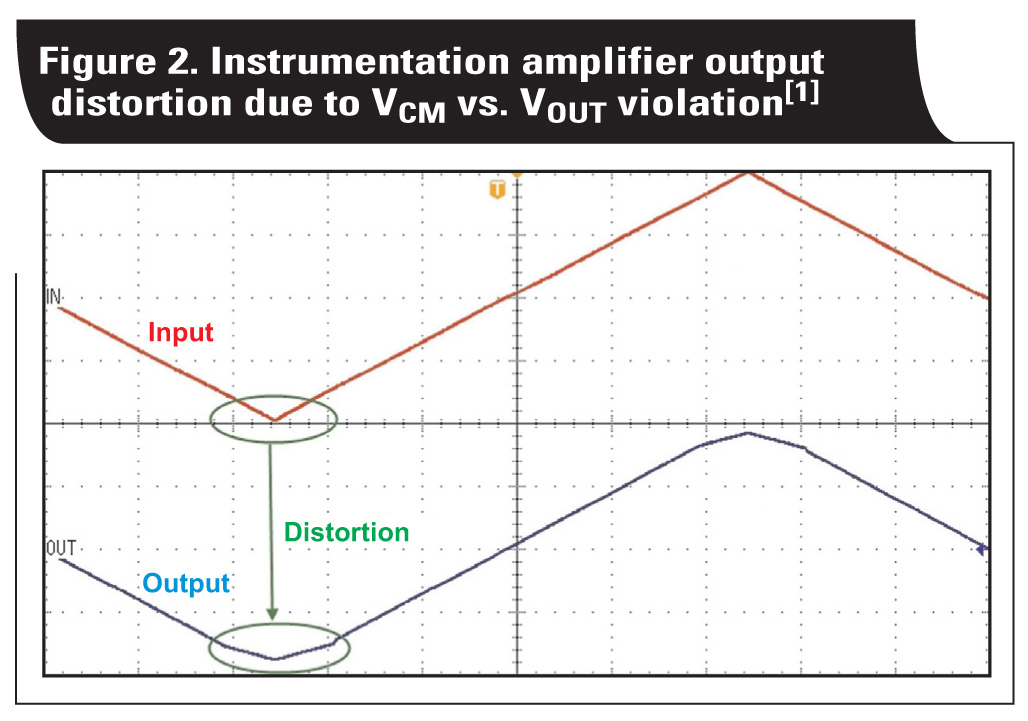
Operating outside the boundaries of a VCM vs. VOUT plot causes the device to operate in a non-linear mode as shown in Figure 2.
A three-part series article and blog post discuss the VCM vs. VOUT plot for the ubiquitous three-op-amp instrumentation amplifier.[1, 2] Two-op-amp instrumentation amplifiers are popular because of their low-cost and relatively large VCM vs. VOUT plots.
Analysis of a two-op-amp instrumentation amplifier
Figure 3 depicts a typical two-op-amp instrumentation amplifier connected to an input signal. This topology has high input impedance and requires only one resistor, RG, to set the gain, which is the same as the three-op-amp topology.
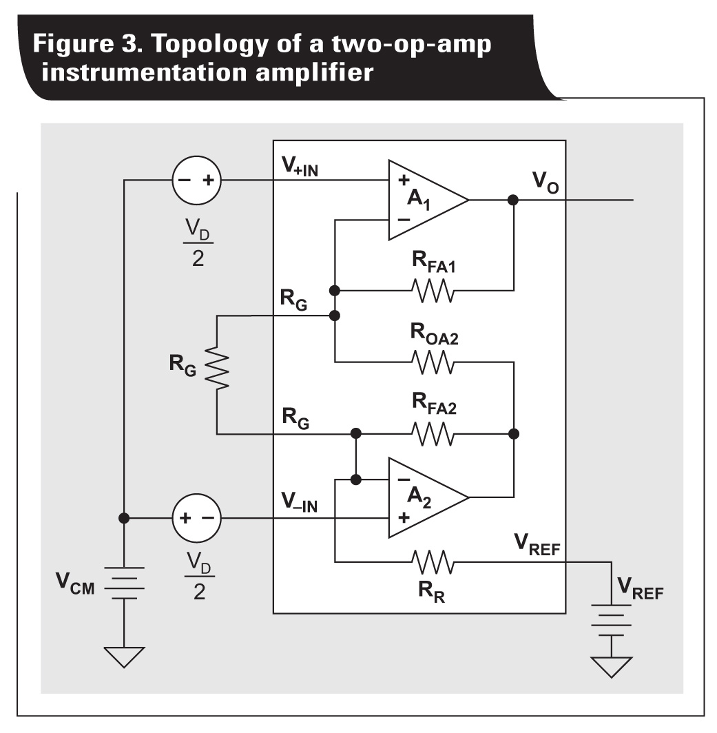
Figure 3 also depicts the definition of common-mode (VCM) and differential-mode (VD) voltages. A differential amplifier (for example, op amp, difference amplifier, instrumentation amplifier) ideally rejects the common-mode voltage, VCM.
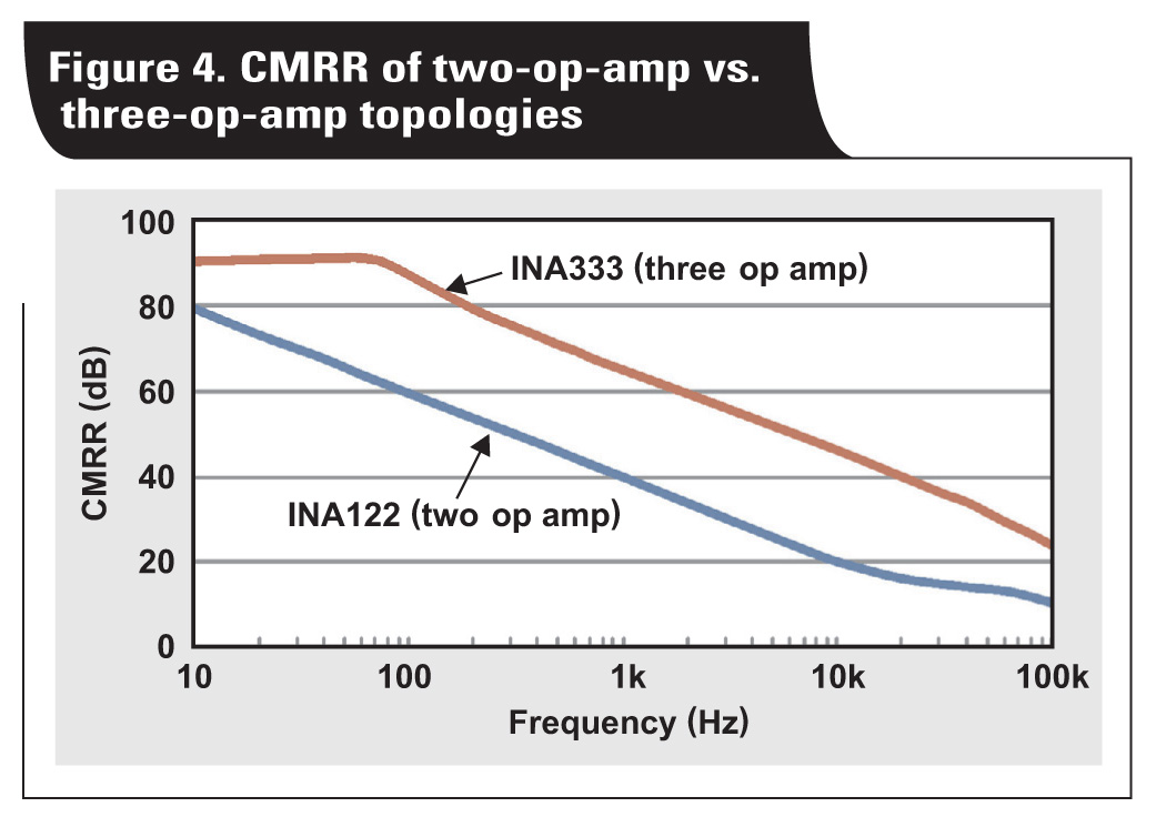
However, the signal-path imbalance from V+IN and V–IN to the output degrades the device’s common-mode rejection ratio (CMRR), especially over frequency (Figure 4). This degradation in CMRR is one of the primary reasons why two-op-amp instrumentation amplifiers typically cost less than their three-op-amp counterparts.
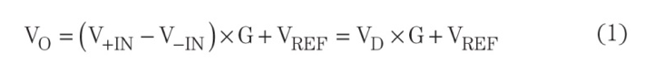
The transfer function for the circuit in Figure 3 is given by Equation 1. Notice that the common-mode voltage does not appear in the equation because ideally it is rejected by the instrumentation amplifier.
Deriving the transfer function of this topology aids in understanding the VCM vs. VOUT plot.
Figure 5 depicts a more traditional drawing of the schematic in Figure 3. In order to determine the contribution of the reference voltage at the output, VO(VREF), apply superposition by shorting the input sources to ground.
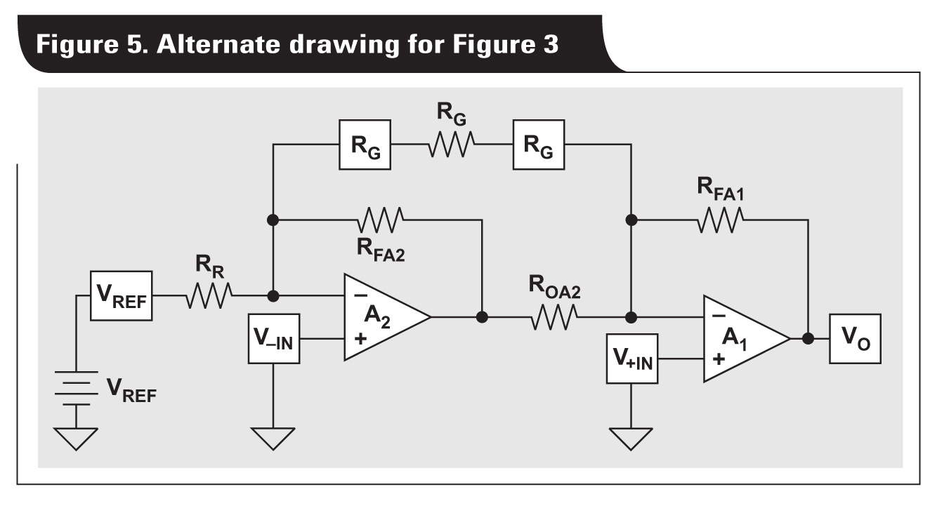
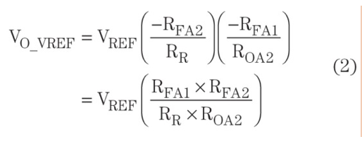
Amplifier A2 applies an inverting gain to VREF based on the ratio of RFA2 and RR. Similarly, A1 applies an inverting gain to the output voltage of A2 based on the ratio of RFA1 and ROA2. Equation 2 depicts the transfer function for VREF.
The gain applied to the instrumentation amplifier’s reference voltage should be 1 V/V. To fulfill this requirement, set RFA1 = RR and RFA2 = ROA2 = RF. Figure 6 depicts the updated two-op-amp topology that results in unity gain for the reference voltage. Furthermore, the internal nodes are labeled for future analysis.
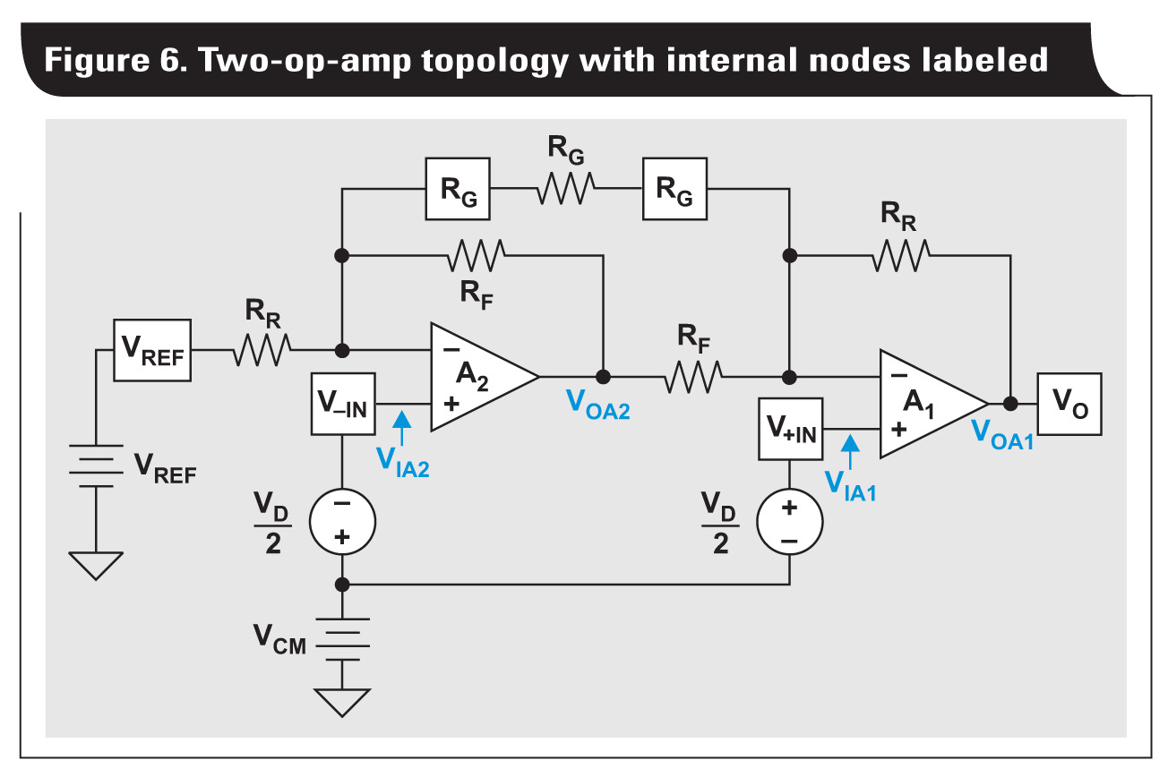
Despite just two amplifiers and five resistors, the circuit in Figure 6 has six gain terms. This is because each amplifier applies gain to three input signals. While it may be obvious that A2 applies gain to V–IN and VREF, A2 also applies gain to V+IN via the virtual short across the inputs of A1 and RG. Similarly, A1 applies gain to VOA2, V+IN, and V–IN. Equations 3 through 8 depict the six gain terms associated with a two-op-amp instrumentation amplifier
Equations 9 and 10 depict the output voltages of amplifiers A1 and A2.
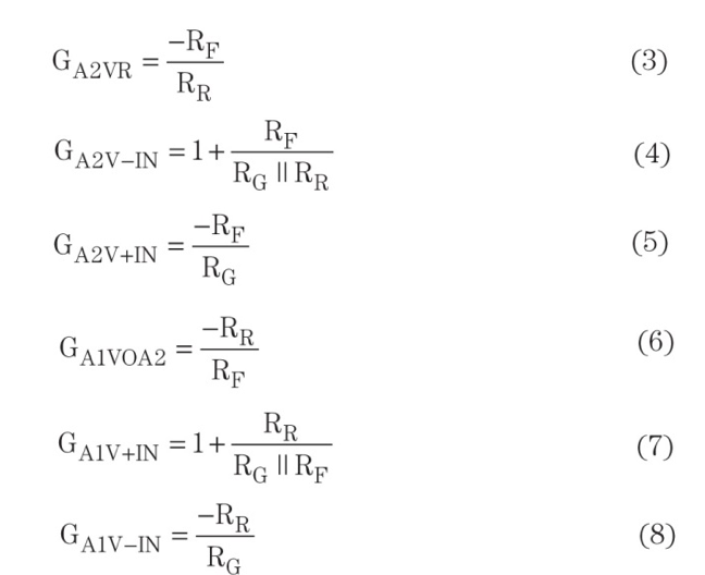
Substituting Equation 10 for VOA2 in Equation 9 and simplifying yields Equation 11.
![]()
The relationship between the gain terms in Equation 11 is shown in Equation 12.
Finally, using Equations 11 and 12, the transfer function for a two-op-amp instrumentation amplifier is shown by Equation 13, which is consistent with Equation 1.
Op amp limitations
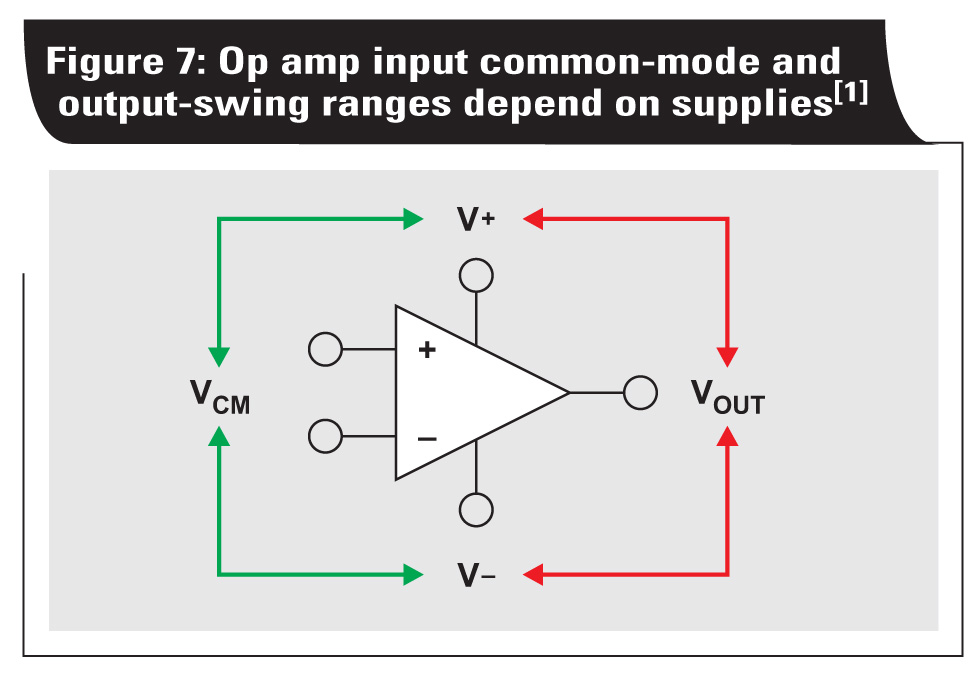
Linear operation of an instrumentation amplifier is contingent upon the linear operation of its primary building block; op amps. An op amp operates linearly when the input and output signals are within the device’s input common-mode and output-swing ranges, respectively. The supply voltages used to power the op amp (V+ and V–) define these ranges (Figure 7).
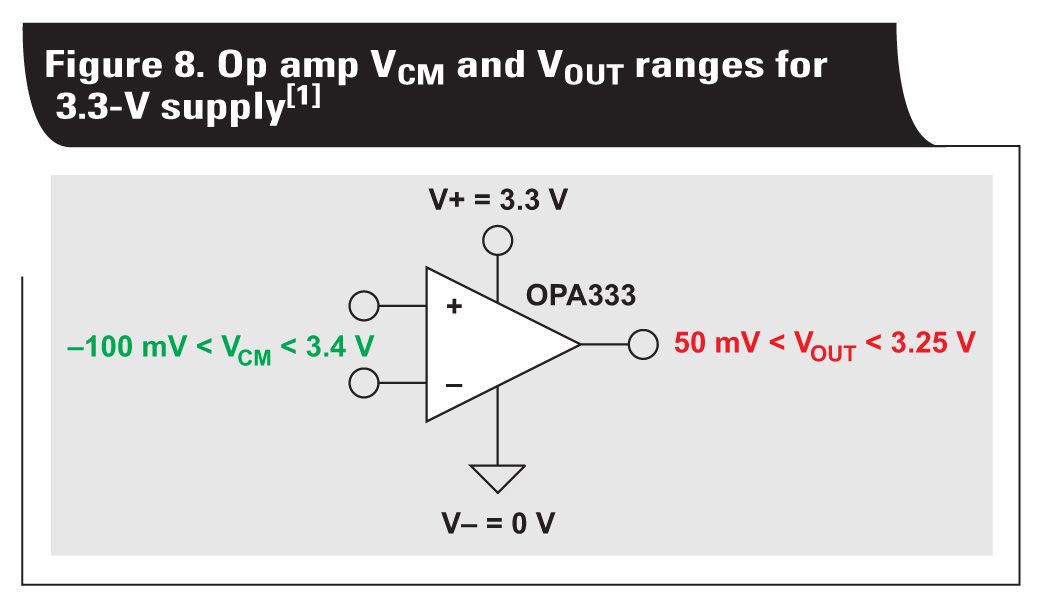
A real-world example of common-mode and output-swing limits is shown in Figure 8. Notice that the common-mode range and output-swing ranges are not necessarily the same.
Two-op-amp node equations
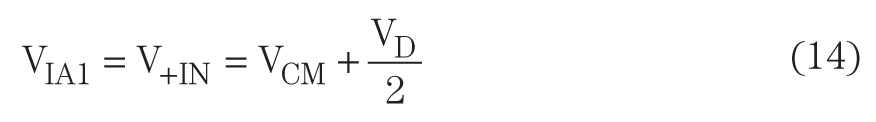
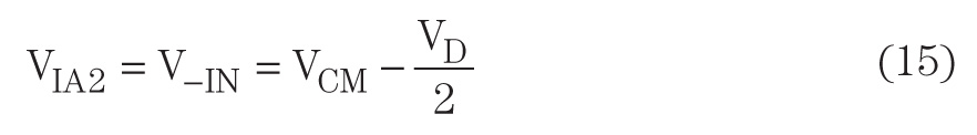
With a solid understanding of the two-op-amp instrumentation amplifier and op-amp limitations, the next step is to examine the node equations as indicated in Figure 6. The equations for VOA2 and VOA1 are already given by Equations 10 and 13, respectively. Equations for VIA1 and VIA2 from Figure 6 are given as:
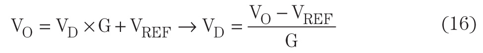
The VCM vs. VOUT plot can vary based on gain and reference voltage. Therefore, Equations 10 and 13 through 15 must be solved for VO as a function of the gain terms, VCM, and VREF. One important relationship that allows for this is obtained by solving Equation 13 for VD, as shown in Equation 16.
After making all of the proper substitutions and solving for VO, Equations 17 through 20 capture the linear operating region of a two-op-amp instrumentation amplifier at its output as a function of the gain terms, VCM, VREF, and the common-mode and output limitations of each amplifier (VIA1, VIA2, VOA1, VOA2).
In order to operate in a linear region, the voltage at VIA1 must not violate the input common-mode range of A1. Similarly, the voltage at node VOA1 must not violate the output swing limitation of A1. The same holds true for VIA2 and VOA2 for op amp A2. The values of the internal op amp limitations are not usually explicitly stated in an instrumentation amplifier’s data sheet. In lieu of such information, a combination of examining the device’s limitations and measuring the linear operating region can be used to determine the values.
To move the input common-mode range closer to the negative supply voltage, some instrumentation amplifiers (for example, INA122) level-shift the inputs using precision transistor buffers.[1] This is particularly useful when operating with a single supply.
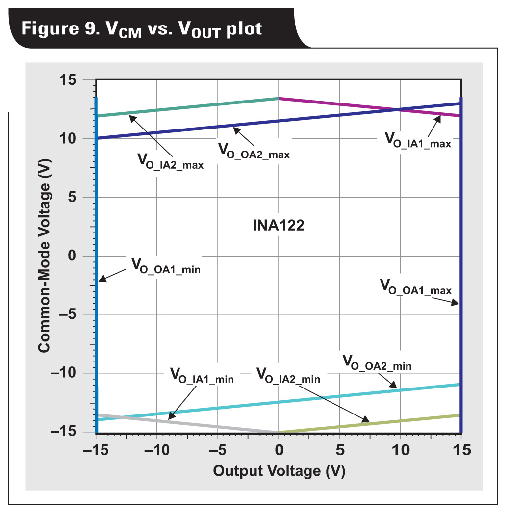
Figure 9 depicts a TINA-TI™ simulation that plots Equations 17 through 20 for both the maximum and minimum common-mode and output-swing limits for the internal amplifiers of the INA122. The linear operating region is the interior of all lines.
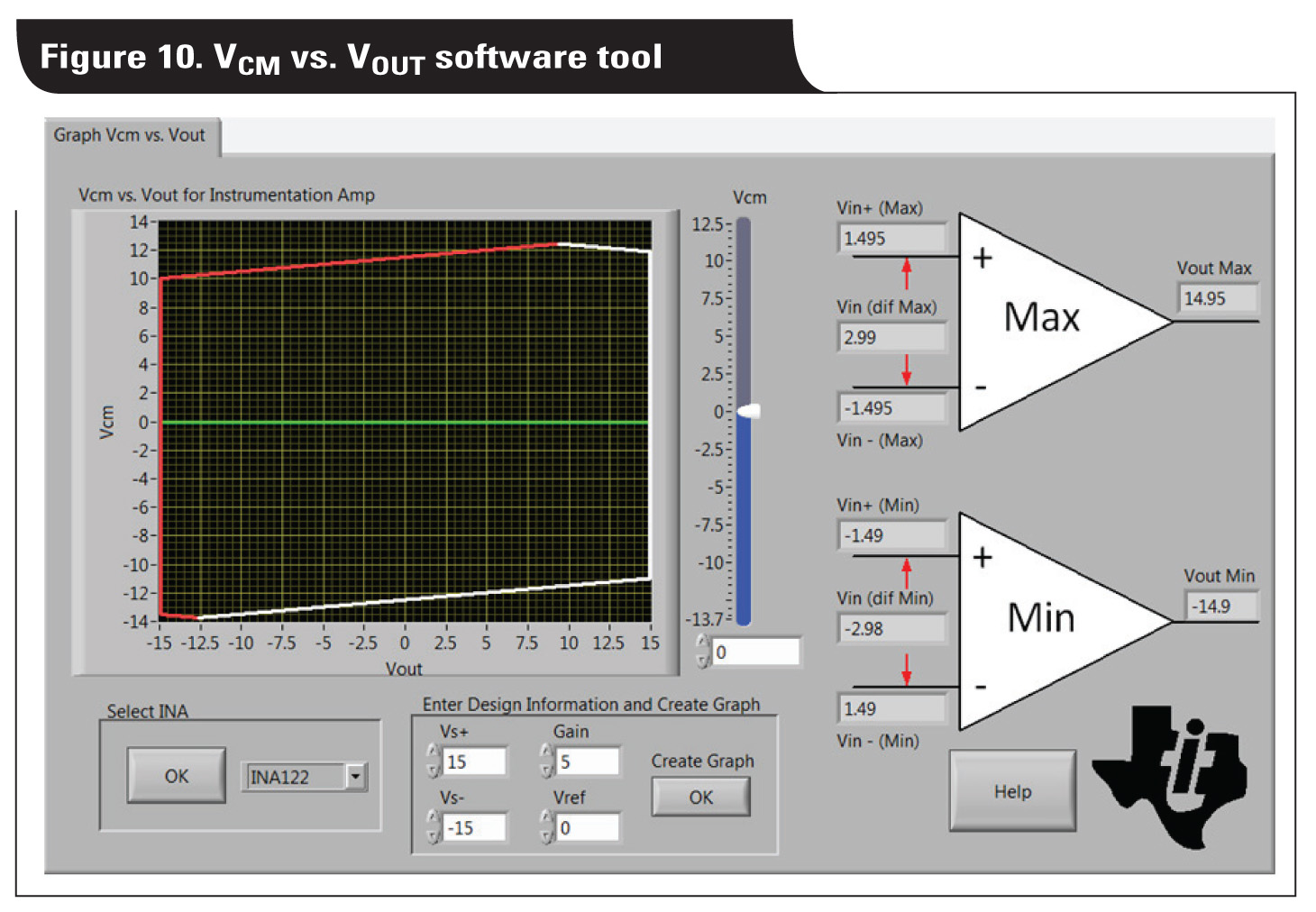
A software tool was developed to simplify the creation of VCM vs. VOUT plots for varying gains, reference voltages, and supply voltages. See Related Web sites an the end of this article for download links. Figure 10 depicts the VCM vs. VOUT plot for the INA122 given standard datasheet conditions. Notice that it compares well with Figure 1 and Figure 9. The datasheet plot in Figure 1, however, only depicts the output limitations of A1 and A2, whereas the software tool includes the common-mode limitations. Finally, note that the software tool can be downloaded to generate VCM vs. VOUT plots for both two- and three-op-amp instrumentation amplifiers.
This article addressed the most misunderstood concept of two-op-amp instrumentation amplifiers: the VCM vs. VOUT datasheet plot. A thorough analysis of the two-op-amp topology was delivered along with the derivation of the internal node equations. These equations were used to create the VCM vs. VOUT plots. The output from the downloadable software tool was found to correlate well with the plot in the INA122 datasheet. This tool gives designers a simple method for ensuring linear operation of the instrumentation amplifier in their design.
Acknowledgements
The author would like to thank Art Kay at Texas Instruments for developing the VCM vs. VOUT software tool and Collin Wells for his technical contributions to this article.
References
- Peter Semig and Collin Wells, “Instrumentation amplifier VCM VOUT plots,” Part 1, Part 2 and Part 3, EDN Network, December 2014
- Peter Semig, “How Instrumentation Amplifier VCM VOUT plots change with supply and reference voltage,” TI Precision Hub, January 30, 2015.
Texas Instruments
www.ti.com