By “Languer“, member on Electro-Tech-Online
This article presents the design of VHF Class-A transistor amplifier intended to provide as much linear output power as possible. It demonstrates basic design techniques to yield optimum output power from a BFR92A bipolar transistor. I based the selection of the transistor upon the following conditions: (1) availability of SPICE model, and (2) availability of S-parameters.
Analysis
To begin the design we need to choose a suitable transistor. For this article, I selected the BFR92A from NXP. This transistor is in no way considered a power transistor; but the availability of SPICE models and S-parameter data allow use of both design non-linear and linear simulation tools. I used LTSPICE and ARRL Radio Designer for the non-linear and linear simulations.
The next step, after transistor/device selection, is to determine a suitable operating point based on desired requirements. The device has a maximum collector-to-emitter voltage (Vce) of +15V and a maximum collector current (Ic) of 25mA. S-parameters are already available for a Vce of +10V and Ic of 20mA. Therefore, I selected this as the desired operating point. The target will be to create the amplifier design for maximum output linear power from 150MHz to 160MHz.
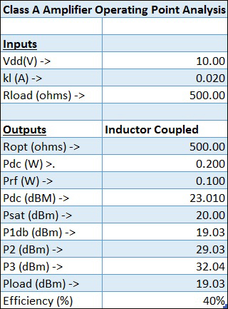
For an inductor coupled design, where most RF power is dissipated on the load (as opposed to resistor-coupled designs) the optimum load impedance is 500-ohms. We determine this by the load line: R_opt = Vce / Ic. You can obtain the parameters below through analysis (along with some empirical “fudge” factors). The table below shows some simple analysis performed using an Excel spreadsheet to calculate the values and expected output power. These are all based on first order approximations; but are indeed very useful to provide some high-level expectations of ballpark performance.
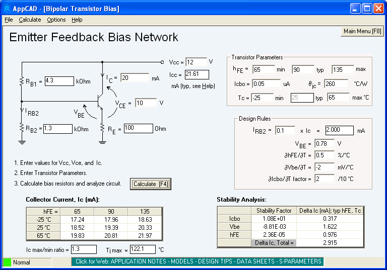
The next step is to select a bias condition circuit given the desired performance and circuit use. For this case, I used AppCad to select and calculate the bias topology and values. The network on the following figure is selected for a few reasons:
- Bias provides good balance for temperature variation.
- Additional current bias resistor on emitter leg can be bypassed at VHF frequencies (note that in most cases it is desired to have the emitter or source legs directly grounded – but for this example having the emitter leg AC grounded should suffice).
- Junction temperature of transistor is kept under control.
Adding the emitter resistor will, however, impact the efficiency since this load absorbs some additional DC power. The following figures show the unmatched amplifier.
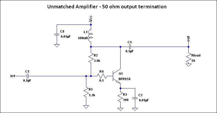
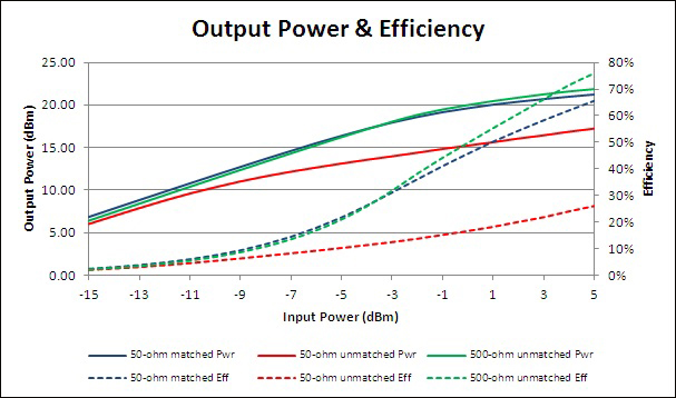
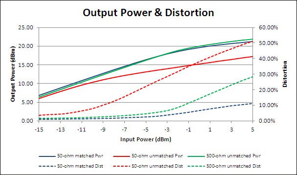
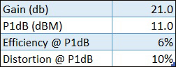
For the amplifier unmatched and driving a 50-ohm impedance (typical for RF and S-parameter measurements) the performance is summarized below:
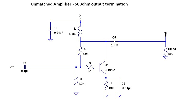
For the amplifier unmatched and driving a 500-ohm impedance (the theoretical ideal impedance for maximum output power) the performance is summarized below:
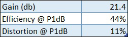
We can make the following observations from the data obtained. The linear gain is quite similar for both configurations. This can be seen as the linear gain is a function of the transistor itself and neither case is really matched for maximum gain. The distortion is quite similar (and not particularly great) for both configurations. This should be somewhat expected because no effort was made to provide any sort of effective match between the transistor intrinsic impedances and the input/output environment. Finally, the linear output power capability and efficiency is much better for the configuration driving the optimum output load (500-ohms), and for the configuration driving a standard (non-optimum) load (50-ohms). Based on the analysis above this is what would have been expected; and the simulation just confirms the analysis.
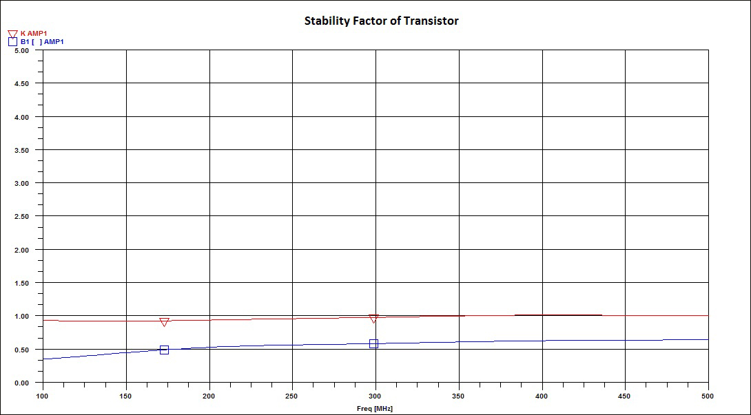
After deciding the bias of the transistor, you can investigate the stability. The following plot shows the stability factor for the transistor under the desired bias conditions. For the transistor to be stable the B1 factor is desired to be above 0, and the K factor is desired to be above 1. In this case the transistor, as biased, is slightly unstable (otherwise known as conditionally stable). Meaning it has the potential to become unstable if the right conditions arise.
Let’s now show the stability circles in order to better understand the stability considerations. These show that most loads (at either input or output) will result in a stable amplifier. There is, however, a small region (for both input and output) where the transistor may become unstable. We can add series or shunt resistance (at either input or output) to stabilize the transistor. Following the circles, the inside of the plot (smith chart) presents all loads which make the transistor input stable over frequency; the inside of the plot also shows all loads which make the transistor output stable over frequency.
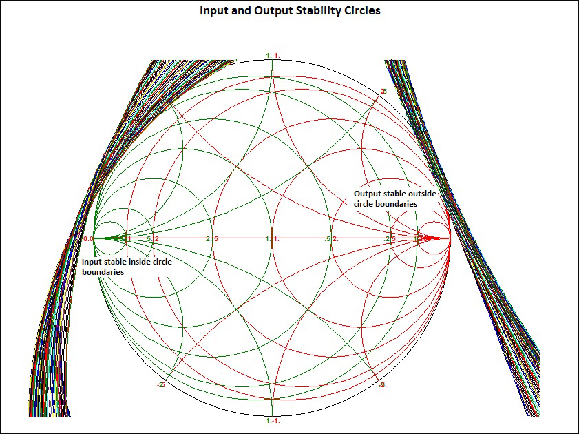
Adding resistance (series or shunt) to either input or output will have an effect on performance. Since in this case the goal is to extract power from the transistor; then the logical compromise is on the input (which will have some impact on the noise figure). From the plot; the resistance line r = 0.1 (red) represents 5 ohms (5 / 50 = 0.1). All the input stability circles are to the right of that line, so if 5 ohms were added to the input; it would “push” the stability circles to the left; and outside the smith chart; effectively stabilizing the transistor over the whole range. The following plot then shows this exact case, where a 5-ohm series resistor has been added to the transistor input. The new B1 and K factors show that the transistor is now stable over the complete frequency range (B1 > 0, K > 1).
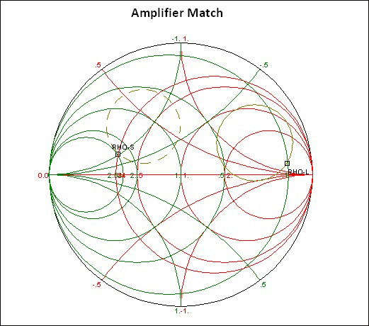
After this, the next step is to provide the desired matching. The desired output load for the transistor is 500-ohms (to maximize the output power capability). But the transistor has an inherent output impedance of 18pF. The goal is then to match the output so the transistor sees 500-ohms and cancels out the 18pF. The label ‘RHO-L’ on the following figure presents this load. Next the conjugate match on the input can be determined by plotting the gain circles (in this case for 20.5dB gain). By plotting the available power circle and selecting the desired load resistance (RHO-L), the corresponding source resistance is given by RHO-S. What does all this means: the output will be mismatched to 500ohms || 18pF to obtain the desired output performance; the input will then be properly matched to what the transistor would like to see to provide the desired output performance.
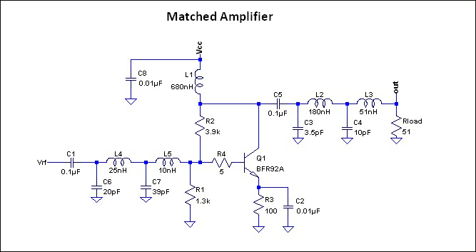
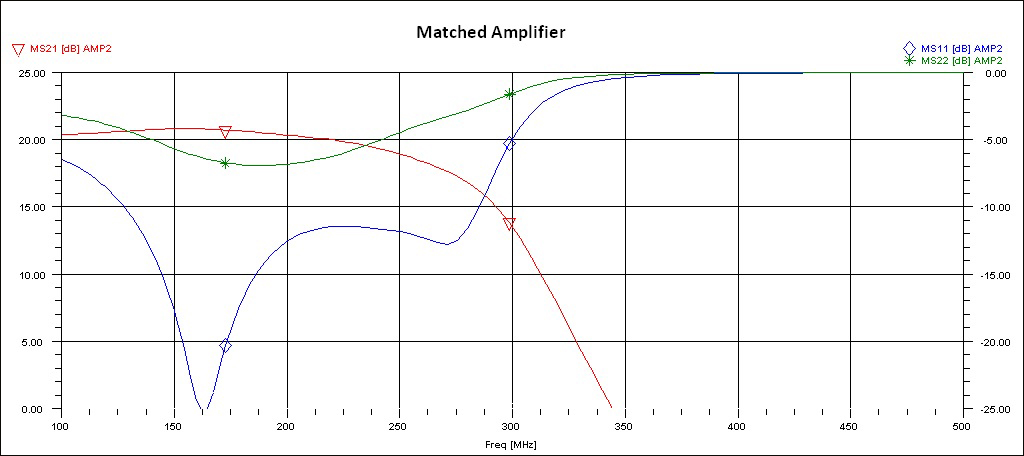
The following figure then represents the final amplifier (matched to input and output to obtain the desired output performance).
And we can observe the gain and match characteristics on the following figure. As expected, the input match is fairly good (better than 15dB), but the output match is not as good (better than 5dB); this is the tradeoff to obtain a specific output performance.
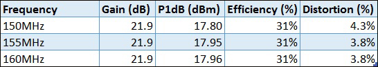
The results are summarized below.
Conclusions
Comparing the results of the matched amplifier (final design) to the results for the unmatched transistor (whether driving 50 or 500 ohms), a few things are evident. The linear output power capability and efficiency are nearly as good for the matched amplifier as that for the one driving the optimum output load (500-ohms) directly. In addition, the distortion is much better for the matched amplifier. The following table and figures summarize the results, showing how the proposed design yields the desired results.
![]()