Semiconductor design complexity has increased exponentially in recent years, and this challenge is exacerbated by the need to collaborate and scale across multiple, globally distributed teams while accelerating time to market. On top of these elements, the industry has been confronted with a major obstacle: the current talent shortage. There is no quick fix to the talent shortage, so companies must figure out how to tame design complexity and meet today’s challenges with the talent they already have.
According to a recent report from Deloitte, the semiconductor industry needs more than 100,000 skilled workers to join the semiconductor workforce per year by 2030. Yet fewer than 100,000 students in the U.S. graduate with electrical engineering or computer science degrees annually. Given this stark talent gap, semiconductor companies must improve efficiencies across the board to do more with their existing resources. This is where an IP-centric design methodology comes into play.
 Currently, most teams employ a traditional project-centric design methodology. This approach worked well when projects were smaller, and teams were physically closer together. Now, this methodology doesn’t work as well for many reasons. First, projects are larger, and timelines are shorter than in previous years. Team members are also more dispersed, requiring teams to collaborate globally with tight coordination. In this new reality, the inefficiencies of project-centric design become apparent. Projects are siloed, so teams end up re-solving the same problems and manually tracking IP and metadata across projects. This lack of coordination from project to project makes it difficult to pool resources, meet compliance requirements, or scale design planning.
On the other hand, IP-centric design creates a centralized system for design management across all types of projects and platforms. This allows teams to reuse IP more effectively, provides end-to-end traceability, and results in unified planning at enterprise scale.
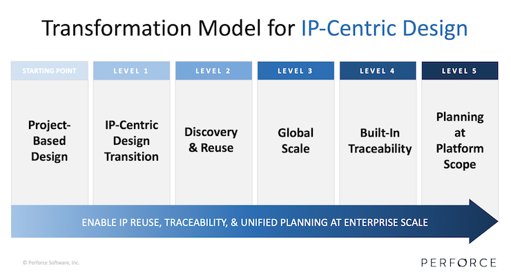
The first step in moving to an IP-centric design methodology is to expand the definition of “IP.” Traditionally, in the context of semiconductor design, IPs were design blocks purchased from 3rd party vendors and delivered to the consumer as opaque, ready-to-use blocks. In the new, expanded definition, any design block — internally developed, externally acquired, specific to a project, or general purpose — is managed as an IP. Even tools and design environments can be considered IPs, allowing the entire project to be a hierarchical collection of IPs that is a complete managed set.
Next, the IPs must be made available to users in a dynamic catalog, allowing users to search and filter for available IPs and then add them as dependencies in their own project. This step is referred to as “discovery and reuse.” The third step is to scale the model for enterprise development effectively. At this stage, the system serves as a central hub of all design-related information. At step four, the system becomes a fully traceable, single source of truth for all of the design’s data and metadata. The fifth and final step in transforming to IP-centric design is planning at platform scope. At this high level, all platform components — whether existing or planned — are modeled in one unified system. This allows teams to better coordinate a project’s upcoming needs, including more informed build-or-buy decisions.
Once organizations have adopted an IP-centric design methodology, true IP reuse is achievable, collaboration is more effective, and design efforts can be streamlined across teams. While IP-centric design can’t outright solve the talent shortage, it can help organizations mitigate the effects of the shortage by boosting the productivity and efficiency of their existing workforce. It can also help teams avoid wasting time “reinventing the wheel” by reusing IP more effectively.