Antenna design and integration is an important activity for 5G telephony, wireless Internet of Things (IoT) nodes, Wi-Fi networks, near-field, and satellite communications, and various other applications. Without robust antenna designs and solid system integration, the performance of those applications can be severely compromised. Balancing the needs for efficiency, gain, bandwidth, pattern characteristics, and decreased sensitivity to the environment while maintaining a development schedule and meeting cost constraints can be a daunting task.
Fortunately, designers have an array of electronic design automation (EDA) tools available for antenna design and integration. This first of two FAQs explores some of those EDA tools. It’s not a comprehensive review but a potpourri of possibilities from component suppliers and test equipment makers. Part two continues with explorations of offerings from general-purpose EDA tool companies and specialized tool makers.
NFC, IoT, GPS, Wi-Fi, Bluetooth, and more
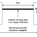
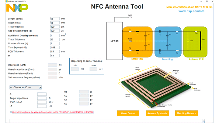
NFC readers need solid antenna designs to ensure proper operation, including optimal read range and reliability. NXP offers its Antenna Design Tool to speed NFC antenna tuning and matching. The process starts with the selection of the NXP antenna being used. The tool automatically provides recommended values for L0 and other filter components based on the synthesis values provided by the user for antenna length and width, track width, gap between tracks, any additional overlap area track thickness, number of turns, turn exponent, circuit board thickness and Epsilon r (εr). In each case, recommended values are provided, but designers can change them as needed for specific design cases. The tool also provides values for the matching network components (Figure 1).
For designers that need cellular, Wi-Fi, GNSS/GPS, LPWAN, or ISM connectivity, Antenova is a source of design tools. Important considerations covered by these tools include best practices for antenna placement, PCB optimization for best RF performance, including component layout recommendations, ground plane space, vias, enclosure materials, and gaps. It also includes guidelines for antenna testing and certifications.
Kyocera AVX also offers a range of design tools for antenna selection and integration in 5G, Wi-Fi, Bluetooth, Zigbee, GNSS/GPS, and ISM applications. It identifies the best antenna for use with popular RF modules from various makers and details 11 best practices for antenna integration and tuning. For example, the IoT Solution Optimizer is designed to speed up the development of reliable NB-IoT solutions for various applications like asset tracking, building management, and machine monitoring. The tools also provide .dxf files for sharing the design results across various computer-aided design (CAD) applications.
MIMO, active beam forming, and phased arrays
Multiple input, multiple output (MIMO) antennas and active beam forming for 5G new radio (NR), radar, satellite, and other advanced antenna systems (AAS) can be designed and modeled using tools offered by Rohde & Schwarz. Beamforming antenna design is complex, but the technology is a standard feature in AAS. The latest designs combine digital beam forming for flexibility and analog beam forming for efficiency, increasing the design complexities. For effective and efficient designs, it’s necessary to identify and compensate for nonlinear characteristics in RF components. Discrete components like phase shifters, switches, and amplifiers need conductive testing. System-level tests and highly integrated frontends with antenna in package (AiP) require over-the-air (OTA) testing. Designers need a range of conducted and OTA design validation solutions.
Designers of AAS can also turn to the W4804B PathWave System Design Core from Keysight, which provides a single platform to architect, design, and verify complex RF systems. This platform is supported in Spectrasys and Dataflow simulators, allowing designers to model RF component behavior and DSP controls accurately. A schematic representation supports the development of RF, digital and hybrid beamforming, and it includes a simple antenna configuration tool for building arrays of varying sizes and configurations. The environment also includes flexible antenna modeling inputs from Keysight’s EM tools and can accept data from third-party software. PathWave System Design also shares data with many RF system engineering tools (Figure 2).

Summary
When developing antenna systems, designers are challenged to meet demanding performance requirements and still satisfy time-to-market and cost constraints. This first of two FAQs presents some antenna EDA tools from component makers and test equipment suppliers. Part two continues the discussion with options from general EDA tool suppliers and specialized tool makers.
References
Antenna Tools, Kyocera/AVX
Finding and integrating an antenna, Antenova
MIMO and active beamforming system design and test, Rohde & Schwarz
NFC Antenna Design Hub, NXP
PathWave System Design Core, RF, Comms/DSP, Phased Array, Keysight