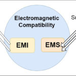
An EMC test is known as Electromagnetic compatibility, a certification for electronic devices to maintain their limitation of electromagnetic waves. As discussed in the previous article, there are two types of EMC tests: emission (EMI) and immunity (EMS). EMI (Electromagnetic Interference) tests measure the magnetic waves emitted by the device, and EMS (Electromagnetic Susceptibility) tests are performed to test emission handling immunity of the device.
This article is about some of the most common EMI tests performed at the EMC test labs on electronic devices. All tests are not suitable for all devices, and an additional test may be required according to the device’s application.
Types of emission (EMI)
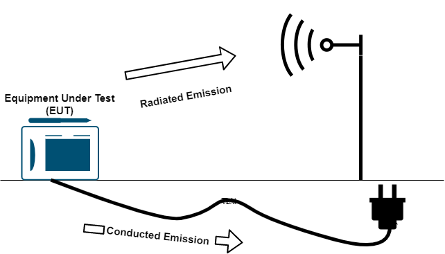
We have already talked about the types of emissions in the previous article. The above image is a diagrammatic representation of those emissions.
Electronic devices may produce any magnetic interference in the environment. Every device emits EMI, but the EMC standards of the country regulate this emission. The regulation can be varied according to different countries. In the USA, EMC standards are defined by FCC (Federal Communications Commission). In, Canada the EMC standard is regulated by Industry Canada.
An EMI test is required to bring a new product to market. This test ensures that the device does not emit any harmful electromagnetic field or harm any other device due to its interference.
Below are some of the most common tests performed by the EMC lab on devices.
- Radiated emission
- Conducted emission
- Flicker
- Harmonic test
Radiated emission
This test involves measuring the EMI in the air that is unintentionally emission generated by the device under test. Because this emission travels through the air, it is called radiated emission.
This is the most common EMC test done by EMC labs worldwide. According to the type of industry, there are certain limitations of radiated emission in the market. Below are some of the different radiated emission testing facilities used by test labs.
➢ Type of radiated emission test sites
The main aim of the radiation emission test site is to measure the radiation that comes from the product and ensure the radiated emission is within the limit. There are two types of test sites used to measure radiated emission. Both test sites are explained below.
- Open Area Test Site (OATS)
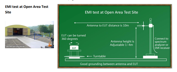
The open area test site is the most common radiated emission test site, also known as OATS.
The distance between the Equipment under Test (EUT) and the antenna is 3m, 10m, or 30m. The measurement distance is crucial because it is a Far Field test, ensuring that distance of measuring the field strength in the far field which is opposite to Near Field. In the near field, the distance between the antenna and EUT is less than the wavelength. In the far field, the distance of EUT and antenna is more than the wavelength.
Labs do not use near field tests because measurement bounces between magnetic and electric fields. The electric field is not stable enough to measure accurate measurements at the near field.
The electromagnetic field varies with distance, so some standards mandate a specific distance separation and some other standards allow to use of two or more lengths to measure radiation emission. The limits are recalculated for each distance.
- Semi Anechoic Chamber (SAC)
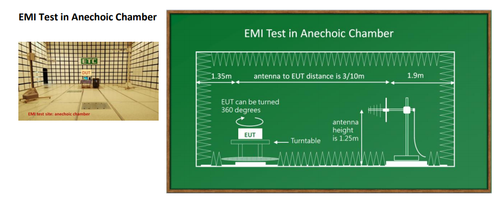
Semi anechoic chamber (SAC) is the same as an open area test site, but it is housed in a shielded room. The enclosure of semi anechoic is made of RF shielded material, and the internal wall is made of absorbing material. An RF shielded enclosure is used to stop external interference, noises, or radio signals. An absorb material is used to prevent echo in signals so that RF signals do not reflect much from the walls. If the RF absorbing material is not present in the room, then the antenna would receive an unquantifiable signal contribution from the wall and ceiling reflections, making measurement entirely inaccurate.
Compared to an open area test site, there is no need to adjust background noises constantly.
Labs mainly use this method because it is a good solution for measuring EMI in a noisy environment.
Radiated emission test setup
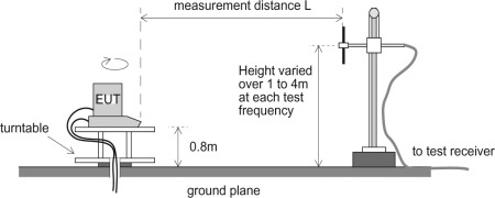
Any product does not produce an Electromagnetic waveform in a spherical pattern. The electromagnetic wave tends to be pretty directional. So test Labs place a product or EUT on a turnable wooden table to measure emission in every direction of the product via rotating the table; also, they vary the height of the antenna between one to four meters for all possible readings.
The ground plane should be covered with an electromagnetic reflective surface (aluminum, steel, wire mesh, etc.), and also the ground plane should be flat, So the Antenna can pick up RF signals direct from EUT, and also it measures reflection from the ground To increase the accuracy in EMI measurement.
Radiated emission limits
The limits for radiated emission depend upon two things country standards and specific application of the device. If the device is made for particular industries, like military, automotive or medical, etc., the emission limits are much stricter and harder to pass the test.
A sample of radiated emission is given below, the blue line is for FCC, and the green line is for Europe. They look very similar, but there is a subtle difference between them. It is possible to pass the FCC but can fail CE emission limits. This plot is from OATS because there is several larger signal in the FM and cell phone bands.
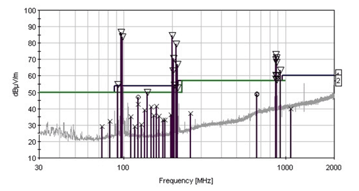
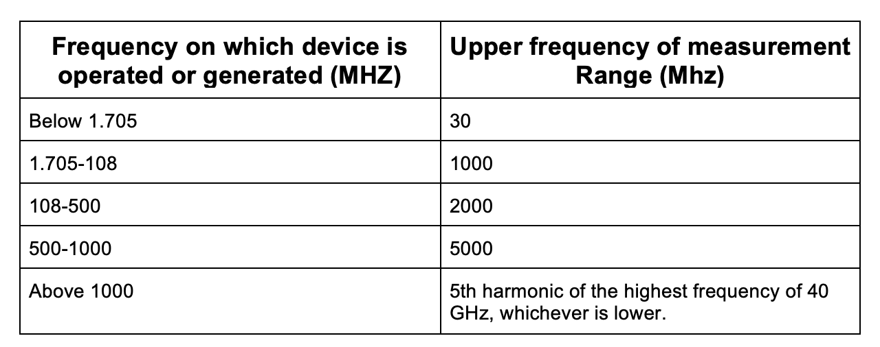
Some of the standards have a fixed frequency of measurement, but the FCC varies the frequency range of measurement according to the device’s frequency.
Measurement antennas for radiated emission
Several types of antenna are used to measure EMI in the lab. Each antenna has a different gain profile across different frequency ranges. Below we show images with different frequency ranges.
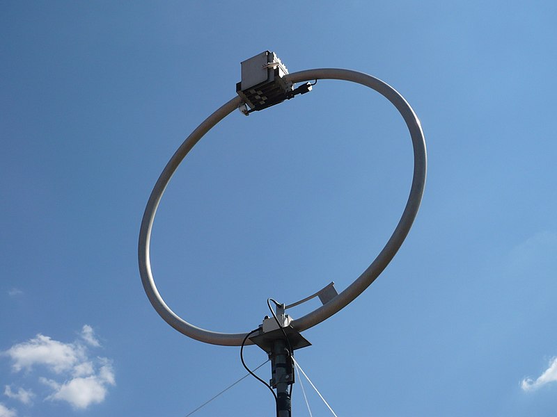
Loop Antenna
Frequency:- 10kHz to 30Mhz
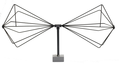
Biconical Antenna
Frequency:- 30MHz to 300Mhz
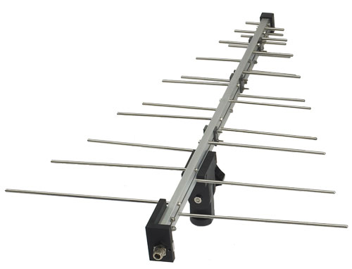
Log Periodic Antenna
Frequency:- 300MHz to 1Ghz
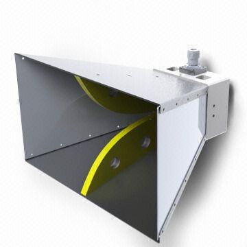
Horn Antenna
Frequency:- 1Ghz to 25Ghz
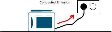
Conducted emission
The interference in the main supply can affect several devices connected to the same main supply. The device generates electromagnetic energy or noise conducted through a power cord, interfering with the power source. This is called conducted emission. Test labs measure these emissions from the frequency range 150Hz to 30Mhz to verify that the conducted emission is within the limit.
Conducted emission testing is performed primarily on the device connected to the AC power supply. Some standard has limits on devices that work on DC power supply.
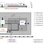
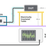
Conducted emission test setup
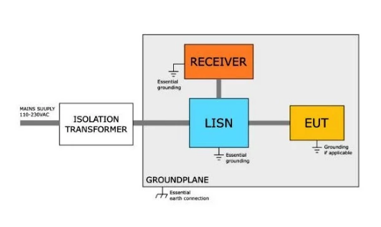
As shown in the diagram above, there is a LISN (Line Impedance Stabilization Network) device.
The LISN device provides a standardized impedance across the EUT measurement points. It couples the measurement point of EUT with the receiver. Also, it prevents unwanted interference signals from going to the other device.
The receiver is a spectrum analyzer that measures the RF signal coming through the LISN device. The LISN and EUT device is placed on the grounded plane.
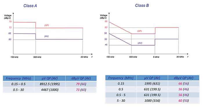
Conducted emission limits
The FCC dictates conducted limits for class A and class B devices. The class B limit is for the domestic environment, so it is more strict. The product must not interfere with other household devices that are already connected.
Flicker and harmonics testing
Harmonics are the distortion of the typical electrical waveform. They are generally transmitted by switch-mode power connectors or other nonlinear like motors, transformers, and lamps.
If there is arcing at the contact point of load that causes a nonlinear current draw, it induces voltage variations that affect nearby lamps. This is called voltage flickering.
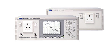
Flicker and harmonic test equipment
Flicker and harmonics can be measured with a low-cost equipment solution.
The TTI (Thurlby Thandar Instruments) can analyze flickering and harmonics associated with a low distortion AC power source.
The circuit below is measures voltage flickering at the terminal of the mains supply. This is the most straightforward block diagram. There is a clean supply source with known impedance used for supply. Any fluctuation or flickering across the terminal of EUT can be measured at the terminal of EUT.
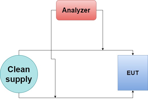
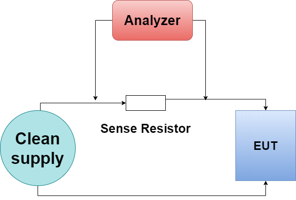
The image below shows the simplest block diagram to measure harmonics across EUT. Similar to the diagram above, a clean supply source is used as a supply of EUT, but there is a sense resistor in series with EUT to measure harmonics current.