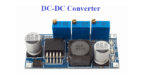
Transition points between PCB traces and wire harnesses impact signal integrity, system-level reliability, and manufacturability. Improperly calibrated transition points can introduce impedance discontinuities, signal loss, or thermal stress. Mechanical strain and layout constraints also restrict routing flexibility, complicate manufacturing, and may contribute to long-term system failures. This article outlines best practices for optimizing PCB-to-harness transition […]
Streamlining PCB-to-wire harness design integration with EDA tools
Automotive wiring harnesses consolidate multiple wires and cables into a single organized system, transmitting power and signals between electronic control units (ECUs). These harnesses connect PCB-mounted electronics to the broader electrical system, supporting advanced driver-assistance systems (ADAS), powertrain control, airbags, infotainment, telematics, and body electronics. This article examines the PCB-to-wire harness design flow and highlights key integration […]
How to select automotive PCB-to-wire harness connectors
An automotive wiring harness routes electrical power and signals between various vehicle components. Within this system, PCB-to-wire harness interfaces use connectors to link discrete wiring bundles with board-mounted electronics. This article explores the fundamentals of PCB-to-wire harness interfaces and outlines connector electrical performance requirements across vehicle platforms. It also highlights the importance of mechanical stability, […]
What are the different stages of PCB design, testing, and manufacturing?
A printed circuit board (PCB) provides the mechanical foundation, electrical interconnections, and signal routing for electronic devices and systems (Figure 1). By enabling compact, reliable, and high-performance circuit integration, PCBs support various industrial, medical, and consumer applications in data centers and at the intelligent edge. This article discusses the three pillars of effective PCB design […]
What are the three types of logic level translators (LLTs)?
Logic-level translators (LLTs) are electronic circuits that enable communication between devices operating at different voltage levels, such as 3.3V and 5V. Also known as voltage-level translators or level shifters, LLTs convert signals between incompatible logic standards. This article outlines key LLT specifications and features, reviewing bidirectional, high-to-low, and low-to-high LLTs. It also explores the role […]
How AI and ML optimize functional verification for EDA
Functional verification ensures that the register transfer layer (RTL) implementation of semiconductor designs operates according to specified requirements. Electronic engineers typically perform functional verification using hardware verification languages (HVLs) such as SystemVerilog paired with the universal verification methodology (UVM). Other HVLs, such as VHSIC Hardware Description Language (VHDL) and Property Specification Language (PSL), may be […]
What is formal verification, and why is it important?
Formal verification uses mathematical analysis to ensure semiconductor designs perform as intended. Typically automated, it efficiently identifies critical design errors, such as deadlocks, race conditions, and unreachable states. This article reviews the fundamentals of formal verification in semiconductor design, explores its integration with simulation for comprehensive validation, and highlights strategies for optimizing implementation. Defining formal […]
Empowering innovation: OpenROAD and the future of open-source EDA
Many electronic design automation (EDA) tools remain out of reach for semiconductor startups and research organizations. However, a growing number of open-source EDA solutions are bridging the affordability gap and democratizing advanced chip design. This article discusses how tools like OpenROAD and OpenLane lower entry barriers, reduce development costs, and drive innovation. It also explores how […]
How hardware-assisted verification (HAV) transforms EDA workflows
Many semiconductor companies rely on hardware-assisted verification (HAV) to optimize sophisticated monolithic system-on-chip (SoC) designs and chiplet architectures. HAV streamlines verification and validation by integrating emulation, field-programmable gate array (FPGA) prototyping, and virtual platforms. This approach enables design engineers to efficiently verify individual components and system-wide interactions while validating functionality at granular and system-wide levels. […]
Parasitic extraction in EDA: what it is and why it matters
Parasitic extraction (PEX) in electronic design automation (EDA) calculates parasitic effects — such as capacitances, resistances, and inductance — within integrated circuits (ICs). Parasitics are introduced during the physical manufacturing process in semiconductor foundries, affecting both IC devices and their interconnects (Figure 1). This article explores the three primary categories of parasitic effects, compares field […]


