While I have covered the basics of noise simulation in SPICE before, I thought it was worth revisiting the subject to show some of the confusing results you can sometimes get and how to interpret them. The example I used earlier, a simple opamp based amplifier, didn’t show any unusual noise results but other circuits can do. The more circuitry you have which affects bandwidth, the more likely you are to see some strange effects, particularly when looking at input referred noise.
A photodiode amplifier — transimpedance amplifier — is probably a good example where you are quite likely to see some strange results. They aren’t that strange when you understand why. You need to include a realistic model of a photodiode. If the circuit is “ideal” and doesn’t reflect reality, then your simulations won’t be very realistic. As always, you need to make sure that your SPICE model simulates the effects of noise – some don’t, and so can be wildly inaccurate.
Take the following example.
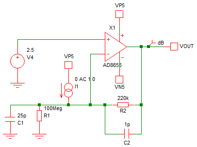
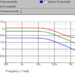
I1 represents a photocurrent with C1 and R1 representing the photodiode capacitance and leakage resistance respectively. C2 provides some stability. Plotting the AC response as well as input and output noise gives the following.
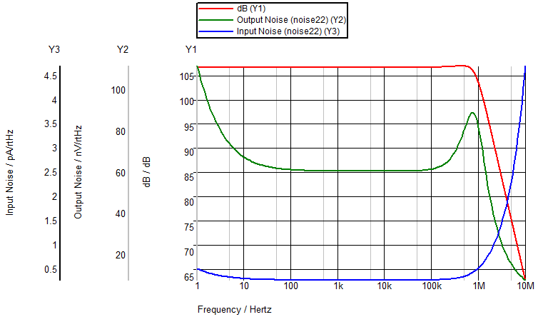
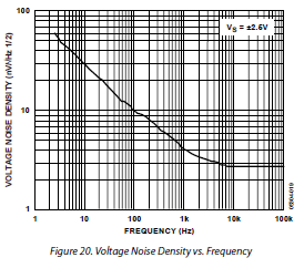
Whether that is what you expected depends on your experience of noise simulations and transimpedance amplifiers. In particular, the peak in output noise around 700kHz might be unexpected as well as the input noise rise from 1MHz to 10MHz (and beyond). The rise in noise at low frequencies is not such a surprise, both on the input and output noise. There are two effects which can cause the rise in noise at low frequencies – current noise and voltage noise. If you look at the voltage noise of an opamp (or almost any active device), you will see the noise rise at low frequencies. For example, for the AD8655 the voltage noise looks like this.
So, a rise is to be expected at low frequencies. There is no graph of current noise versus frequency for the AD8655, although that would only have a significant effect on a large feedback resistor. You might notice that the noise of the opamp starts to increase below around 10kHz but in the transimpedance amplifier circuit it doesn’t start to rise until well below 100Hz. The reason for this is that the output noise is dominated by R2, the feedback resistor, in the mid-frequency range. You can check this by plotting the R2 noise against the output noise.
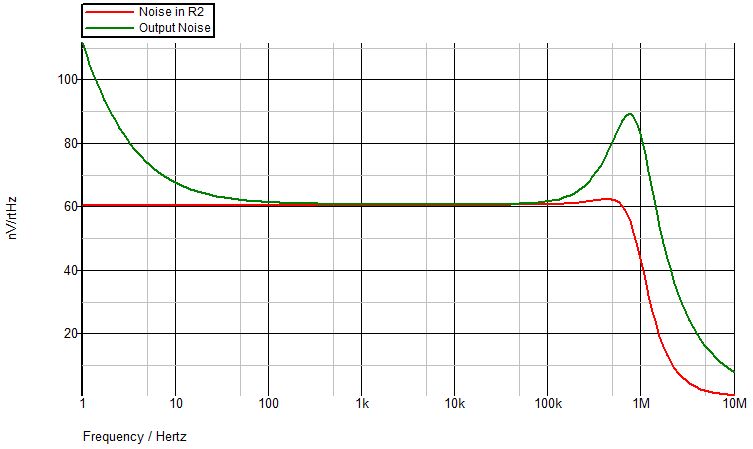
Ideally, I would also plot the opamp noise, but sometimes my simulator doesn’t like to plot the noise of subcircuits. However, you can see that output and R2 noise are almost identical from 100Hz to 100kHz, so no other component is adding much to the total noise.
So, what about the massive rise in input noise above 1MHz? Well, you need to be careful when looking at input referred noise. Output noise is in some ways a better thing to look at, although input noise is also useful when interpreted correctly. If the output noise is low, why is the input noise high (at 10MHz, for example)? The answer is that it isn’t! Input noise is really “input referred” noise. A circuit is full of noise sources (many within the opamp), and they contribute to the final output noise by differing amounts depending on where they are in the circuit and the amount of noise. So, something creating noise near the input could then have its noise multiplied considerably by the time it reaches the output. A noisy device near the output may have little effect. All these noise sources are summed with their respective gains to arrive at the final output noise graph.
To create an “input referred” noise graph the output noise is divided by the transfer function to produce a graph of what the input noise would have to be like if it all came from the input (even though it doesn’t). In this case, the circuit has very little gain at 10MHz, but there is still some noise. Some math may help to understand it. At 1kHz the output noise is 60.6nV/rtHz. The “gain” (transimpedance) is 107dB. Dividing 60.6nV by the 107dB (and remembering that the source is a current, not a voltage) results in 271fA/rtHz. If you measure the input noise on the simulation, it is 275fA/rtHz so about the same. Note that simulations showing “dB” for the gain, in this case, can be misleading because it is really a conversion of current to voltage. So, 20dB means 10A/V, not 10V/V. So, 107dB means around 224mV/µA, to keep the numbers to something more realistic.
So, what about 10MHz? The gain at 10MHz is 64.3dB and the output noise 7.74nV/rtHz. Dividing the output noise by the gain results in 4.7pA/rtHz which is exactly what the simulation shows. However, this gives an unrealistic impression of the real noise because it is only really the output noise that is of importance.
What about the peak in the output noise near 1MHz? Well, unfortunately, that is real. All output noise effects are likely to be real unless they are caused by model or circuit errors. You can find a thorough analysis of noise in transimpedance amplifiers in the Texas Instruments Application Bulletin SBOA060 (previously a Burr-Brown document). You need to look at the “noise voltage gain” of the circuit. The noise voltage of the opamp in a transimpedance amplifier is not usually too important – the noise is dominated by the feedback resistor voltage noise and possibly the opamp current noise. However, the voltage noise of the opamp is amplified such that the noise increases with increasing frequency depending on the values of R1/R2/C1/C2.
A “perfect” transimpedance amplifier with an ideal photodiode would have no noise gain. The capacitance of the photodiode would be zero and the leakage resistance infinite. However, a real circuit has a noise gain based on R1/R2/C1/C2. This is plotted below for the example circuit.
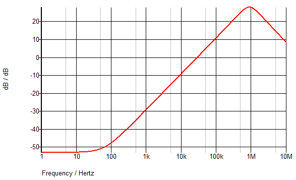
The gain is quite low at low frequencies, but as the frequency increase, C1/C2 start to influence the gain until it peaks when the circuit bandwidth starts to reduce it again. So, at its peak, you will be amplifying the opamp voltage noise by 28dB, and this will be added to whatever noise is there due to other components such as the feedback resistor, and also the opamp current noise. With 2.7nV/rtHz from the amplifier and 60nV/rtHz from a 220k resistor, the opamp noise would appear insignificant. However, multiply the 2.7nV by 28dB peak noise gain, and you get 68nV/rtHz. Add this to the resistor noise (using sum of squares), and you arrive at 91nV/rtHz – almost the same as the peak value shown in the output noise simulation.
The noise peak is determined by C1 and C2, and you can move the peak around and push it higher in frequency by changing the capacitors. Unfortunately, the feedback capacitor is needed for stability and C1 is the photodiode capacitance. Reducing the bandwidth will reduce the gain, but often you want the maximum speed possible. If you can reduce the photodiode capacitance, then you can reduce the noise peak, and another technique for reducing the noise is to bootstrap the photodiode to reduce the effective capacitance.
Want a summary?
1. noise simulations are useful, but you need to be careful how you interpret the input noise,
2. simulations are no substitute for understanding how the circuit works and where the noise comes from.