• Skip to primary navigation
  • Skip to main content
  • Skip to primary sidebar
  • Skip to footer

Analog IC Tips

Analog IC Design, Products, Tools Layout

  • Products
    • Amplifiers
    • Clocks & Timing
    • Data Converters
    • EMI/RFI
    • Interface & Isolation
    • MEMS & Sensors
  • Applications
    • Audio
    • Automotive/Transportation
    • Industrial
    • IoT
    • Medical
    • Telecommunications
    • Wireless
  • Learn
    • eBooks / Tech Tips
    • FAQs
    • EE Learning Center
    • EE Training Days
    • Tech Toolboxes
    • Webinars & Digital Events
  • Resources
    • Design Guide Library
    • Digital Issues
    • Engineering Diversity & Inclusion
    • LEAP Awards
    • Podcasts
    • White Papers
  • Video
    • EE Videos
    • Teardown Videos
  • EE Forums
    • EDABoard.com
    • Electro-Tech-Online.com
  • Engineering Training Days
  • Advertise
  • Subscribe

IoT front end module designed in adherence to Thread and Matter

January 10, 2024 By Redding Traiger Leave a Comment

pSemi Corporation announced the introduction of their smallest PA-LNA-SW Internet of Things (IoT) front-end module (FEM): the PE562212. Designed in adherence to the Thread and Matter protocols, industry frameworks that focus on simplifying connected experiences, PE562212 is an ultra-compact multi-protocol 2.4 GHz FEM that enables a variety of connectivity options for IoT devices.
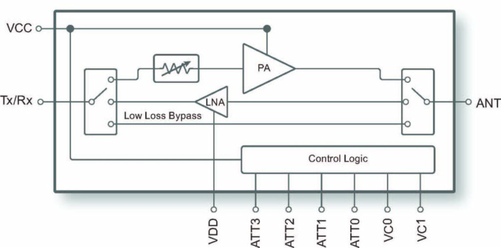
With a 14-lead 1.8 × 1.8 × 0.7 mm LGA package (MSL3), the PE562212 is an IoT FEM specifically designed for space-constrained applications, delivering superior flexibility and value to IoT device makers. The PE562212 enables connectivity across Thread, Zigbee, Bluetooth BR/EDR, BLE, and low-medium throughput Wi-Fi (MCS7) as well as 2.4 GHz proprietary applications. It can be used to connect everything from smart speakers, smart lighting, smart thermostats, and in-home appliances to IoT hubs, range extenders, wireless audio, wearables, sensors, asset tracking, industrial devices, and more to ensure link robustness.
The new IoT FEM is designed with both efficiency and linearity in mind as it enables higher data rate applications such as Wi-Fi, striking the delicate balance of adequate linear power with that power efficiency. Powered by pSemi’s proprietary UltraCMOS technology, PE562212 leverages high-performance capabilities and integration for PCB-limited IoT applications with up to +21 dBm output power and digital Tx gain control of 1 dB steps with 15 dB range. It also delivers industry-leading Rx capability (1.5 dB NF, typ.) and low IL bypass path (0.9 dB, typ.) with a GPIO control interface.
PE562212’s ultra-compact design provides PCB space savings and easier board routing as no external SMD components, including control lines, supply lines, and RF, are required. It also offers excellent ESD and ruggedness for all intended applications and environmental conditions inherent to the IoT space.
Samples and EVKs for PE562212 are available now, directly through pSemi, and are expected to be commercially available by August 2024.

You may also like:


  • Where are cloud connected relays used?

  • What’s a digital shadow and how does it relate to…

  • How do digital threads & digital twins fit in MBSE?

  • What materials can be used to make miniature antennas?

  • What can you make with MEMS technology?

Filed Under: Audio, Industrial, IoT, Products, Tools, Wearables, Wireless Tagged With: psemi

Reader Interactions

Leave a Reply Cancel reply

You must be logged in to post a comment.

Primary Sidebar

Featured Contributions

Design a circuit for ultra-low power sensor applications

Active baluns bridge the microwave and digital worlds

Managing design complexity and global collaboration with IP-centric design

PCB design best practices for ECAD/MCAD collaboration

Open RAN networks pass the time

More Featured Contributions

EE TECH TOOLBOX

“ee
Tech Toolbox: Connectivity
AI and high-performance computing demand interconnects that can handle massive data throughput without bottlenecks. This Tech Toolbox explores the connector technologies enabling ML systems, from high-speed board-to-board and PCIe interfaces to in-package optical interconnects and twin-axial assemblies.

EE LEARNING CENTER

EE Learning Center
“analog
EXPAND YOUR KNOWLEDGE AND STAY CONNECTED
Get the latest info on technologies, tools and strategies for EE professionals.

EE ENGINEERING TRAINING DAYS

engineering

RSS Current EDABoard.com discussions

  • Rolling Code Tx-Rx nano module
  • Spot welder - parallel connection of MOFTET
  • Bandgap reference low power design doubts
  • Need clarification on SWDIO/SWCLK length‑matching and “shielding” for STM32WBA5MMG debug connector
  • Question recap electronics

RSS Current Electro-Tech-Online.com Discussions

  • analog logic of shmidt trigger bjt circuit
  • Unable To Get Advertised Op-Amp Slew Rate
  • Micro mouse
  • Best practices for accurate LiPo battery monitoring on ESP32?
  • Flip Flop for My Mirrors
“bills

Footer

Analog IC Tips

EE WORLD ONLINE NETWORK

  • 5G Technology World
  • EE World Online
  • Engineers Garage
  • Battery Power Tips
  • Connector Tips
  • EDA Board Forums
  • Electro Tech Online Forums
  • EV Engineering
  • Microcontroller Tips
  • Power Electronic Tips
  • Sensor Tips
  • Test and Measurement Tips

ANALOG IC TIPS

  • Subscribe to our newsletter
  • Advertise with us
  • Contact us
  • About us

Copyright © 2026 · WTWH Media LLC and its licensors. All rights reserved.
The material on this site may not be reproduced, distributed, transmitted, cached or otherwise used, except with the prior written permission of WTWH Media.

Privacy Policy