A combination of optics, lasers, electronics, and combined with advanced physics principles, allows “touch-free” physical manipulation of molecules, viruses, and other nano-sized objects.
How do you manipulate and move tiny objects such as pieces of DNA or living cells? Conventional mechanical or vacuum tweezers, no matter how small, couldn’t grab them and would cause damage even if they could, while AFMs (atomic force microscopes) aren’t suitable, either.
Instead, you can use an optical tweezer, formally known as a “single-beam gradient-force trap”, which uses a specially focused laser beam (there they are, again, solving problems) to precisely hold and direct tiny objects as small as a few hundred nanometers with pico-newtons of force. [Note that when the optical laser was first demonstrated in 1970, some pundits derided it as “a solution in search of a problem to solve”; it turns out that they were correct, and in more ways, than they ever could have imagined!]
A team developed the optical-tweezer innovation at Bell Labs in the late 1970s, and the dimensional scale of their use has since been extended down in range from handling individual proteins, viruses, and bacteria strands to enabling trapping and manipulation of neutral atoms. This feat was closely related to the award of a Nobel Prize in Physics in 1997 to Steven Chu, William Daniel Phillips, and Claude Cohen-Tannoudji “for development of methods to cool and trap atoms with laser light.”
Note that the term “optical trapping” is often associated with “optical tweezer” and “optical tweezing,” as trapping – namely, catching and holding – the object of interest before it can be moved and manipulated. The optically driven nanoscale technology of optical tweezing is even being investigated for other applications such as allowing photons to directly control a MEMS electrical switch, thus forming a fast, integrated optical-electronic interface.
Physics principles control the show
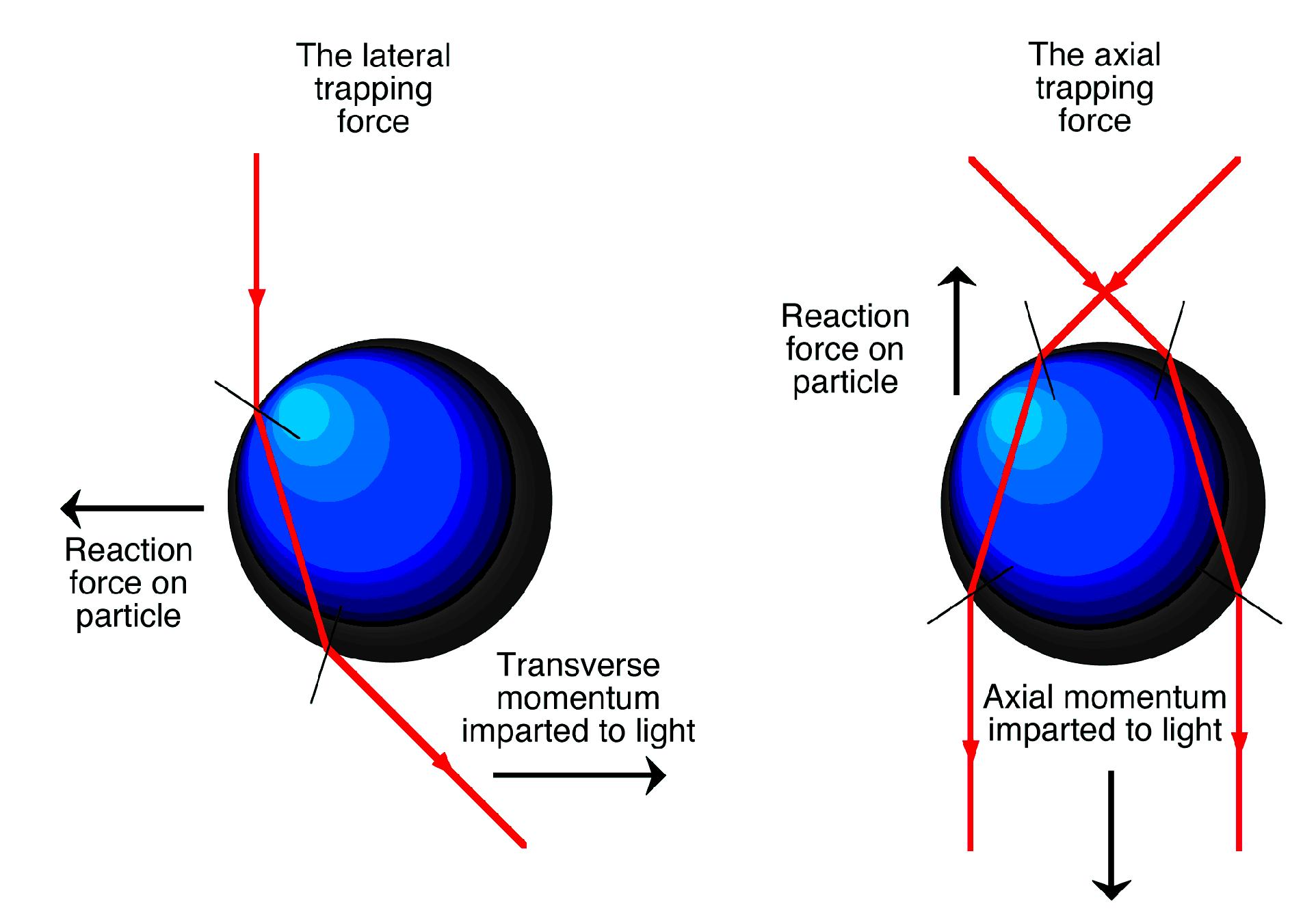
This article will present a math-free, minimal-physics discussion of the optical tweezer, but there is no denying that both the math and physics are intense. Optical tweezers are based on the long-established understanding of optical-radiation pressure. Still, it is much more complicated than just shining one or more intense beams of focused laser light at the object to be manipulated, in order to trap it or push it along.
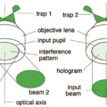
The first major step toward a practical optical tweezer was presented in a four-page paper by Arthur Ashkin (Reference 1), where he describes how he and his team were able to trap dielectric spheres in three dimensions by using a combination of radiation from two counter-propagating but unfocused laser beams plus the force of gravity. In these experiments, they were able to overcome the effects of random, thermally induced motion (Brownian motion), which otherwise overwhelmed any control via optical-radiation pressure, and actually observe the basic trapping effect (Figure 1).
Ashkin received the Nobel Prize in 2018 “for the optical tweezers and their application to biological systems,” eleven years after Chu, Phillips, and Cohen-Tannoudji, whose work was based on his efforts. (At age 96, Ashkin was the oldest Nobel Laureate until 2019 when Roger Goodenough, 97, was awarded the Nobel Prize in Chemistry for his work on lithium-ion batteries.)
But trapping is not the same as achieving control and motion. Ashkin demonstrated in 1986 that a system with just a single, focused laser beam and a gradient lens could do more: it could act as a controllable “tweezer” to grab and move the trapped object at will. In theory, the laser power only needs to be a modest 1 mW, although in practice, a beam between 5 and 10 milliwatts is used to compensate for path losses and beam imperfections—still a fairly low-power beam.
Part 2 of this article examines the underlying optical-physics principles in more detail and begins building up to a complete system.
EE World References
Assembling Micro-Components With Laser Tweezers
Nanotweezer Is New Tool To Create Advanced Plasmonic Technologies
A Levitated Nanosphere As An Ultra-Sensitive Sensor
The difference between scanning electron microscopes and tunneling scanning electron microscopes
The instrumentation of nanotechnology
Magnetic resonance imaging (MRI), Part 1: How it works
MRI, Part 2: Historical development (and lawsuits)
Nanowires As Sensors In New Type Of Atomic Force Microscope
Atomic Force Microscope Reveals Chemical Ghosts
External References
- Ashkin, A., “Acceleration and Trapping of Particles by Radiation Pressure,” Physical Review Letters, 1970. 24(4): p. 156
- Justin E. Molloy and Miles J. Padgett, “Lights, action: optical tweezers,” (Contemporary Physics), 2002, volume 43, number 4, pages 241 to 258.
- Trygve Bakken & Adam Koerner, “Optical Tweezers,” University of California at San Diego, Biophysics Lab, June 2009.
- “Optical trapping: How does it work?, University of St. Andrews, Scotland.
- Stanford University, “An introduction to optical tweezers”
- Arvix.org (Cornell University), “Step-by-step Guide to the Realisation of Advanced Optical Tweezers”
- Harvard University, “Inexpensive optical tweezers for undergraduate laboratories”
- Review of Scientific Instruments, “Optical Trapping” (via Semantic Scholar)
- Wikipedia, “Bessel beam”