Controlling noise in analog and mixed-signal circuits is important but not simple. Data integrity is dependent on controlling noise in the signal chain. If left uncontrolled, noise can impair or disrupt system operation. This FAQ starts by looking at the various sources and types of noise, looks at how noise can enter the signal chain through various components, considers printed circuit board grounding and layout techniques to help control noise, and reviews some design techniques for controlling noise.
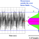
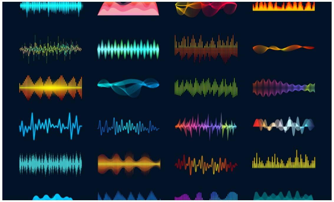
Noise can be caused by various sources and manifests in a range of frequencies, bandwidths, and spectrum distributions (Figure 1). Noise can take the form of common-mode or differential-mode energy. It can originate within the system or come from outside sources. Whatever its specific characteristics or source, noise is an undesirable form of energy.
Sources and types of noise
There is a range of noise sources in analog and mixed-signal systems. Some common types of noise include white noise, pink noise, Johnson noise, quantization noise, and popcorn noise.
White noise has a flat spectrum and is distributed uniformly throughout the frequency domain. Bandwidth reduction can be used to remove white noise from an analog signal. Reducing the bandwidth of an amplifier by a factor of N reduces RMS white noise by the square root of N.
Pink noise, also called flicker or 1/f noise, has a frequency dependence inversely proportional to frequency. The energy of pink noise at each frequency level falls off at about 1 to 3 dB per octave. This is in contrast to white noise which has equal energy at all frequency levels. As a result, pink noise is strongest at low frequencies, but at higher frequencies, it loses strength, and white noise becomes the primary source of noise. Eliminating pink noise can be challenging at the PCB level.
Johnson noise, also called thermal noise, is the random excitation of electron motion that is a function of temperature. Johnson noise is unavoidable and can only be completely eliminated at zero degrees K.
Quantization noise is a result of errors introduced by quantization in an analog-to-digital converter (ADC). It’s non-linear and signal-dependent. It’s caused by the rounding error between the analog input voltage to the ADC, and the output digitized value.
Popcorn noise, or burst noise, which is low frequency and the result of imperfections in devices. It’s random and, therefore, unpredictable.
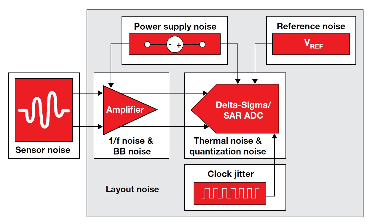
Various sources of noise are inherent in electronic components and combine into a noise figure for the inputs and outputs. A noise analysis can determine the noise level, called the noise floor, below which any signal will be indistinguishable. The noise floor for an interconnect or component is defined by the input noise from all sources, the bandwidth of the component or circuit element, and the noise figure of the interconnect or component. Noise can enter the signal chain through various components such as:
- ADCs, which produce thermal and quantization noise.
- Amplifiers, which produce broadband and 1/f noise
- Voltage references, which produce broadband and 1/f noise
- Clocks, which produce jitter.
- Power supplies, especially switch-mode converters, which produce a variety of periodic and random noise types
- Printed circuit board (PCB) layouts that couple noise from external sources into the system.
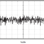
- Sensors, which contribute a wide variety of noise types into sensitive systems (Figure 2).
Noise can be produced in the PCB by current spikes that occur on some signals. In analog circuits, these spikes are often caused by changes in load current, while in digital circuits, current spikes result from transistor switching. Noise can also result from an incorrect ground or floating ground connection. Grounding is especially important. A simple single ground point is often enough in PCBs where the maximum signal frequency is 1MHz or less. A star or multipoint ground architecture is often needed if higher frequencies are involved. Some designs combine a single point ground for low-frequency blocks and a multipoint ground scheme for high-frequency blocks.
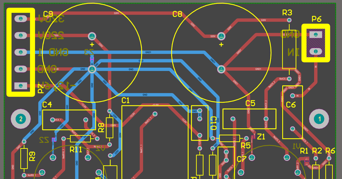
Component placement is also important when minimizing PCB noise sources and levels. Some common recommendations include:
- Placing power components close together on the same layer reduces inductances created between the via holes.
- Arrange high-frequency components to minimize trace lengths as much as possible.
- Place decoupling capacitors as close as possible to the power pins, reducing current spikes from signal switching and minimizing ground bounce back. A rule of thumb with multilayer ceramic capacitors (MLCCs) for decoupling is to use 0.1 µF MLCCs for frequencies up to 15 MHz and 0.01 µF MLCCs for higher frequencies.
Given the numerous types and sources of noise, it’s important to be proactive in reducing and controlling noise in analog and mixed-signal designs. Common recommendations include:
- Use high-order filter circuits when needed to control noise outside the desired bandwidth. Filtering can be used to control analog sources of noise and control the digital signals’ rise/fall times.
- Specify devices such as comparators with rise times no faster than needed to reduce high-frequency harmonics.
- When using an ADC for sampling, noise can be spread across a wider bandwidth and total noise reduced by using a higher sampling rate followed by an anti-aliasing filter.
- Noise from amplifiers can be reduced by specifying devices that have no more than the necessary bandwidth, when necessary, filtering can be added to decrease the effective bandwidth.
Summary
Noise is an undesirable fact of life in analog and mixed-signal circuits. Noise comes from various sources and in a range of energy signatures or formats. It can enter the signal chain through a variety of mechanisms. A noise analysis can determine the expected noise level, called the noise floor, in a given design, below which any signal will be indistinguishable. Designers have a range of tools available to control the impact of noise on system performance.
References
Fundamentals of Precision ADC Noise Analysis, Texas Instruments
Removing Noise From Analog Signals in Your PCB, Altium
Top 5 Rules for PCB Noise Reduction, Proto-Electronics