
Analog functions like sensor interfaces, signal conditioning, power management, and energy harvesting are needed in many applications. These functions are implemented with circuits like operational amplifiers, regulators, filters, sense amplifiers, low-noise amplifiers, phase-locked loops, analog-to-digital converters (ADCs), mixers, analog receiver front ends, and so on. These functions complement digital processing and can be implemented as separate analog ICs, or as mixed-signal ICs that combine the analog and digital sections.
This FAQ begins with a review of some of the challenges of designing analog ICs, looks at modeling tools based on IEEE standards, and how they are being adapted to development environments to speed up the design process. It closes by looking at an effort to develop a universal framework for analog IC development.
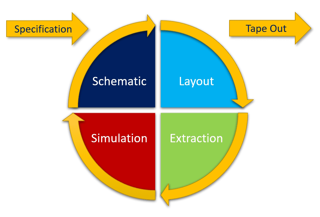
Analog IC designers must deal with multi-dimensional optimization problems for parameters like gain, bandwidth, signal distortion, noise sensitivity, power supply sensitivity, and temperature effects. As a result, while the analog section in a typical mixed-signal IC may occupy only 20% of the chip area, it can demand over 40% of the design effort. Compared with digital IC design that’s highly automated, the design process for analog ICs is more challenging, and it can be a circular and iterative process (Figure 1).
Standardized modeling
The first step toward automating analog IC design is having a standardized modeling framework. The IEEE Std 1666.1-2016, also called the SystemC AMS standard, is a commonly employed option and introduces system-level design and modeling of embedded analog/mixed-signal (AMS) systems. Using the SystemC AMS extensions results in a uniform and standardized modeling approach at higher levels of abstraction. SystemC AMS extensions can also be used together with digital and SystemC design methodologies. They can support exploring various architectural approaches, functional modeling, and virtual prototyping of AMS systems and applications. SystemC AMS is built on top of the SystemC core language, that is, in turn, built on top of C++ (Figure 2). That provides a good foundation, but more is needed to speed up the AMS design process.

Speeding up the design iterations
There are numerous efforts underway to speed up the analog IC design process. In one case, a template-based generator approach and a SystemC AMS pipeline ADC model were combined into an executable toolchain. Using this approach, layout-aware performance estimates of a configurable capacitive pipeline ADC can be computed in a runtime of about one minute per iteration.
The input parameter set was used to configure the template (number of device rows) and the model parameters like non-ideal capacitors and operational amplifier offsets. Estimates of layout parasitics can be calculated in about 5 seconds, and the complete pipeline ADC can be calculated in about 50 seconds. Once the ‘best’ solution has been identified, it takes about one minute to generate the capacitor layout (Figure 3).

Universal design automation framework for analog integrated systems
The National Science Foundation (NSF) is funding the ‘universal design automation framework for analog integrated systems’ project to advance the field of analog design automation (ADA) tools. According to the NSF, there’s a need for an ADA solution that combines versatile system-scale handling, reliability, and the optimal level of human interaction. Today’s tools are deemed too ‘ad-hoc’ and require an excessive amount of human intervention. The project is expected to identify a pathway to breakthrough ADA performance. As defined by the NSF, it will consist of three primary areas of research:
- Development of an innovative unified analog system modeling method, which can describe a wide range of analog systems in the form of linear filter models built from a common set of basic operation cells. This method includes an intelligent synthesis algorithm and a user interface to aid designers in turning their thoughts into models.
- Development of a soft cell concept, which performs on-the-fly circuit creation for the operation cell. This idea will address the reliability issue through a software-hardware co-design methodology.
- Development of an early performance prediction mechanism that guides designers to achieve better results.
A practical biomedical system-on-chip design will be used to validate the resulting framework and demonstrate circuit performance comparable with similar commercial devices. The demonstration project will include interdisciplinary activities of modeling, circuit design, and algorithm development. It’s expected to be based on knowledge bridges between the circuit design and EDA communities to leverage closer collaboration and co-development.
Summary
Analog IC EDA tools are not as automated as their digital IC counterparts. That may change. There’s already a standard modeling process available in the SystemC AMS modeling extensions. Numerous efforts are underway to streamline the analog IC design process, including some that are building on top of the SystemC AMS model, and there’s a new effort by the NSF to develop a universal design automation framework for analog ICs.
References
A Multi-level Analog IC Design Flow for Fast Performance Estimation Using Template-based Layout Generators and Structural Models, Fraunhofer
Continuous integration for analog ICs, Pulsic
Design Automation for Analog Circuits, Technical University of Munich
SystemC Analog/Mixed-Signal Extensions, SystemC
Universal Design Automation Framework for Analog Integrated Systems, National Science Foundation
What is analog design?, Synopsys


