
Antenna design and integration is an important activity for 5G telephony, wireless Internet of Things (IoT) nodes, Wi-Fi networks, near field and satellite communications, and a range of other applications. Without robust antenna designs and solid system integration, the performance of those applications can be severely compromised. Balancing the needs for efficiency, gain, bandwidth, pattern […]
Featured
If you are working with antennas, here are some tools to consider, Part 1

Antenna design and integration is an important activity for 5G telephony, wireless Internet of Things (IoT) nodes, Wi-Fi networks, near-field, and satellite communications, and various other applications. Without robust antenna designs and solid system integration, the performance of those applications can be severely compromised. Balancing the needs for efficiency, gain, bandwidth, pattern characteristics, and decreased […]
The Radio Data System: FM radio adds features to stay viable, part 4

Broadcast FM radio has extended its user-friendly capabilities through the addition of embedded, backward-compatible functionality which adds text and even graphics to the radio display. This part concludes with additional RDS details and IC implementations. Q: Where is the RDS signal in the FM-channel spectrum? Does it affect existing FM stereo broadcasts? A: One of […]
The Radio Data System: FM radio adds features to stay viable, part 3

Broadcast FM radio has extended its user-friendly capabilities through the addition of embedded, backward-compatible functionality which adds text and even graphics to the radio display. RDS is part of FM radio’s effort to maintain relevance and meet user expectations in the face of many alternative ways in which users can access news, music, and more […]
The Radio Data System: FM radio adds features to stay viable, part 2

Broadcast FM radio has extended its user-friendly capabilities through the addition of embedded, backward-compatible functionality which adds text and even graphics to the radio display. This part looks at other radio-receiver upgrades that preceded RDS. Q: Is this the first time that FM radio has been “upgraded”? A: No, not at all. In the 1970s, […]
The Radio Data System: FM radio adds features to stay viable, part 1

Broadcast FM radio has extended its user-friendly capabilities through the addition of embedded, backward-compatible functionality which adds text and even graphics to the radio display. From the late 1920s and for decades afterward, AM-based broadcast radio was the primary real-time mass media in the US and the world. In the AM band (550 kHz to […]
FAQ on fractal antennas, Part 2

Antennas based on fractal mathematics offer some significant advantages but also some controversy. The first part of this article looked at the basic concept and history of fractals. This part looks at the relationship between fractals and antennas. Q: All this fractal discussion is interesting, but what does it have to do with antennas? A: […]
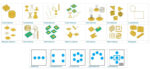
FAQ on fractal antennas, Part 1

Antennas based on fractal mathematics offer some significant advantages but also some controversy. Although all antenna designs are derived from either the basic dipole or monopole/ground-plane configurations, there are almost countless antenna variations in use (Figure 1). Each one offers a different combination of key attributes such as center frequency, bandwidth, bandwidth, side lobes, front-to-back […]
Zero-drift amplifiers finesse ultralow-frequency signals, Part 3
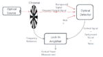
Modern zero-drift amplifiers provide the extremely low drift and noise performance, needed for processing many optical biological, and physical-world signals near 0 Hz. Contrary to what you might think, mechanical chopping is still alive and useful. Given the outstanding performance of electronic components, using a high-performance zero-drift amplifier seems the way to go. That is […]
Zero-drift amplifiers finesse ultralow-frequency signals, Part 2
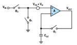
Modern zero-drift amplifiers provide the extremely low drift and noise performance needed for processing many optical biological, and physical-world signals near 0 Hz. The ultimate limitations of chopping led designers to investigate another approach called auto-zeroing, which is especially feasible with integrated circuits. This is a dynamic correction technique that works by sampling and subtracting […]